EHWA DIAMOND – since 1975
Wafer machining from rough grinding to polishing
EHWA coordinates diamond grit, bond and pore structure with the requirements of the particular wafer. This complete family edition covers vitrified NANOPOL tools, resin and metal-bonded versions, sapphire and SiC applications, microblades and dicing blades, and subsequent dry polishing. The programmes differ by material, grinding stage, machine configuration and target surface.
Z1 denotes rough grinding and Z2 fine grinding. In the polishing examples, Z3 denotes the subsequent polishing stage. Grit designations and EHWA specification codes are retained. Identical technical content is presented together; different ranges, codes and test conditions have separate tables. The documented results describe specific applications and support technical selection.
The chapters connect stock removal, consistent tool load, reduced edge chipping, surface quality and die strength. Particularly thin silicon wafers and compound structures incorporating copper, moulding compound, polyimide and solder require coordinated tools and process stages. Start with the workpiece material, then consider the machine, mounting, initial and target thickness, and available machining time.
Editorial version: 13 October 2026. This date identifies the editorial compilation.
Compound wafers: programme and technology
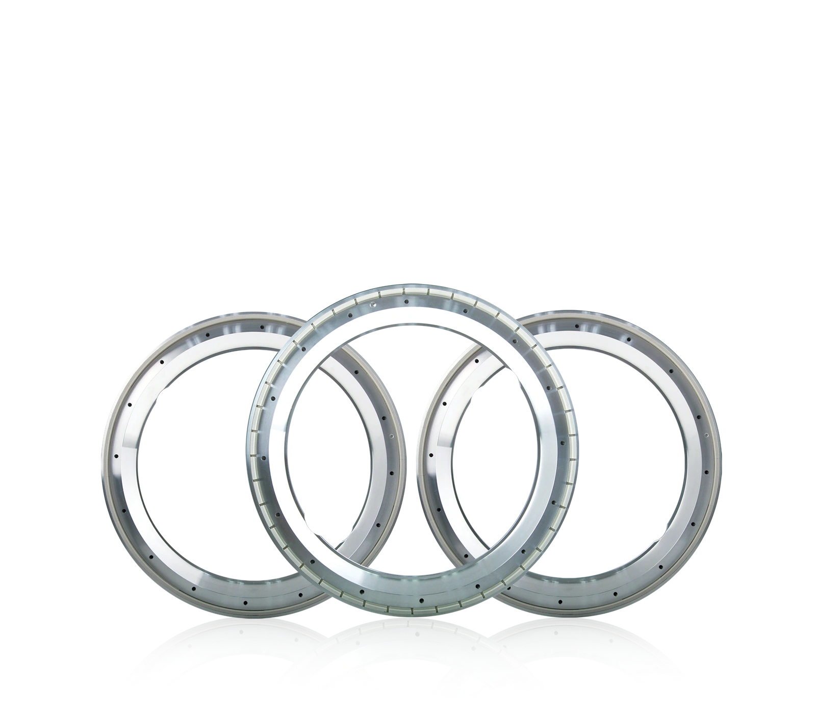
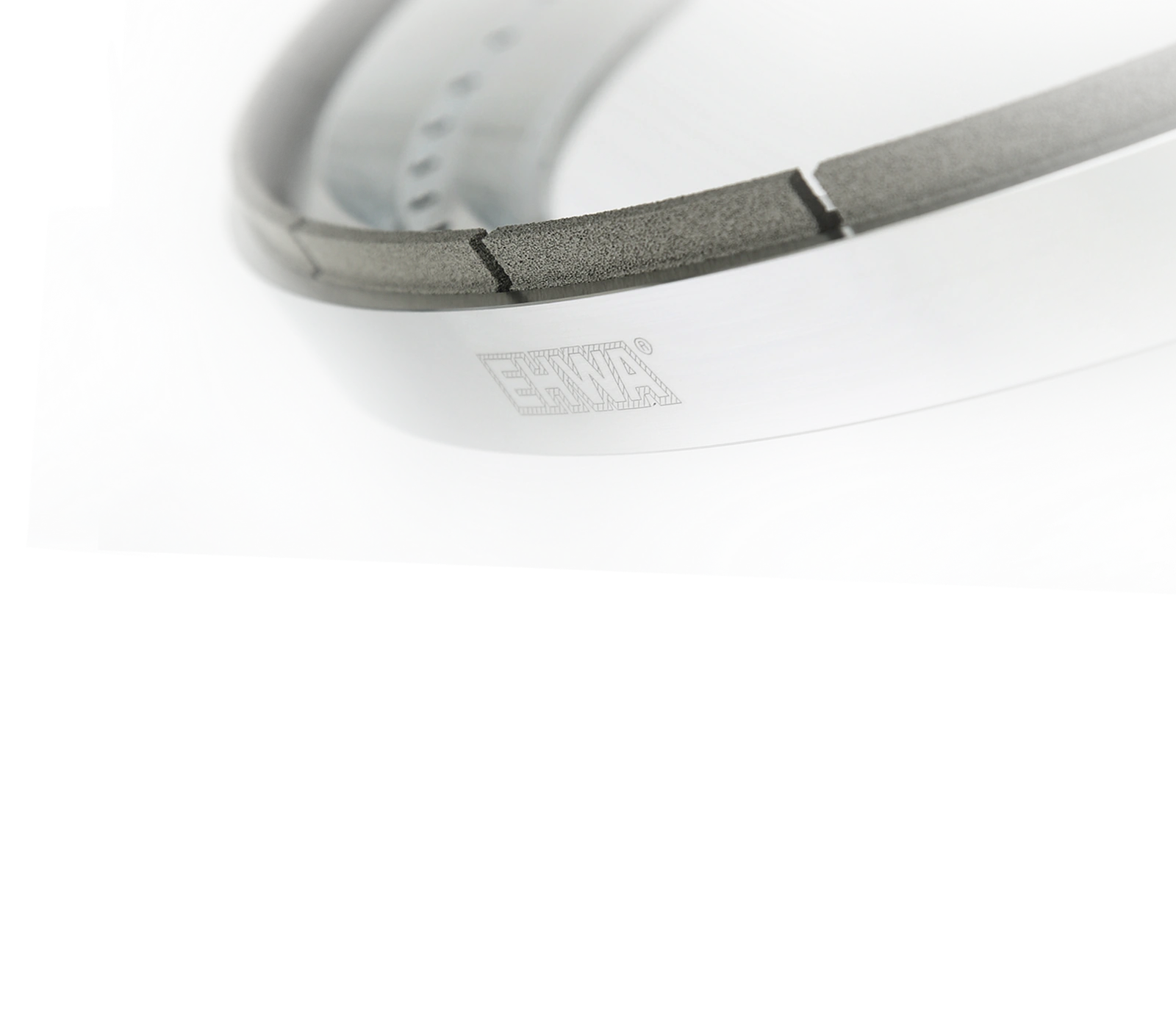
The selection matrix distinguishes Z1 rough grinding from Z2 fine grinding up to polishing level. In the matrix, #400, #600, #800 and #1000 are in the Z1 range; #2000, #3000, #4000, #5000 and #6000 are in the Z2 range. The following ranges reproduce the highlighted series coverage.
| EHWA series | Highlighted grit range |
|---|---|
| VSP Series | #400 to #6000 |
| VSBT Series | #800 to #3000 |
| VSPS Series | #2000 to #6000 |
| VK8B | #5000 to #6000 |
| VK8HS | #3000 to #6000 |
EHWA describes the following NANOPOL features and application capabilities:
- Surface roughness and die strength can be improved through suitable wheel and process design.
- Grinding stress and wafer edge chipping can be reduced.
- Diamond distribution within the grinding segment can be made consistent.
- Porosity, pore shape and pore size can be adjusted.
- EHWA describes processing ultra-thin silicon wafers down to 17 µm thickness. The underlying process conditions are not fully specified in this catalogue; achievable thickness is assessed for the actual application.
- The compound designs are described for TSV and conventional compound wafers, including the fingerprint applications mentioned in the document.
These features describe design capabilities. They do not replace wheel selection for your specific wafer composition.
Grinding mechanism: silicon and adhering material constituents
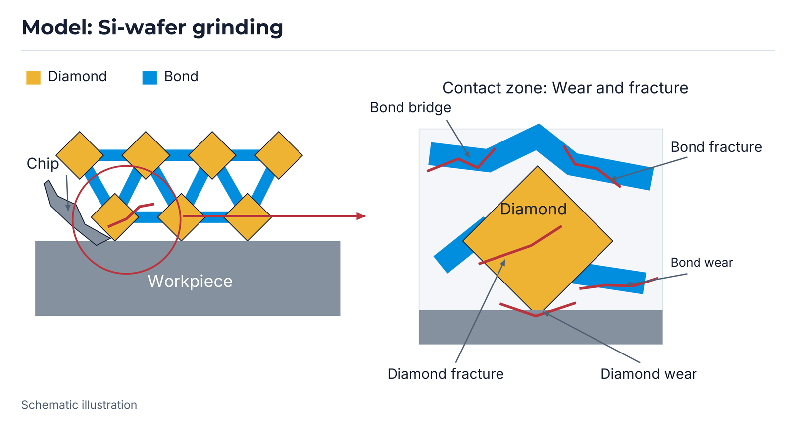
The EHWA silicon grinding diagram shows chip formation together with diamond grain and bond wear and fracture. Renewal of the grinding surface exposes further diamond grains. The interaction between diamonds, bond bridges and pores supports continued material removal.
With adhering material constituents, this surface renewal may be insufficient. The EHWA diagram shows a ductile material adhering to the grinding surface. The renewal mechanism described for silicon therefore cannot be transferred unchanged to every compound structure. Grain and bond wear also depend on the process when grinding ductile materials; adhesion does not mean these mechanisms are universally absent.
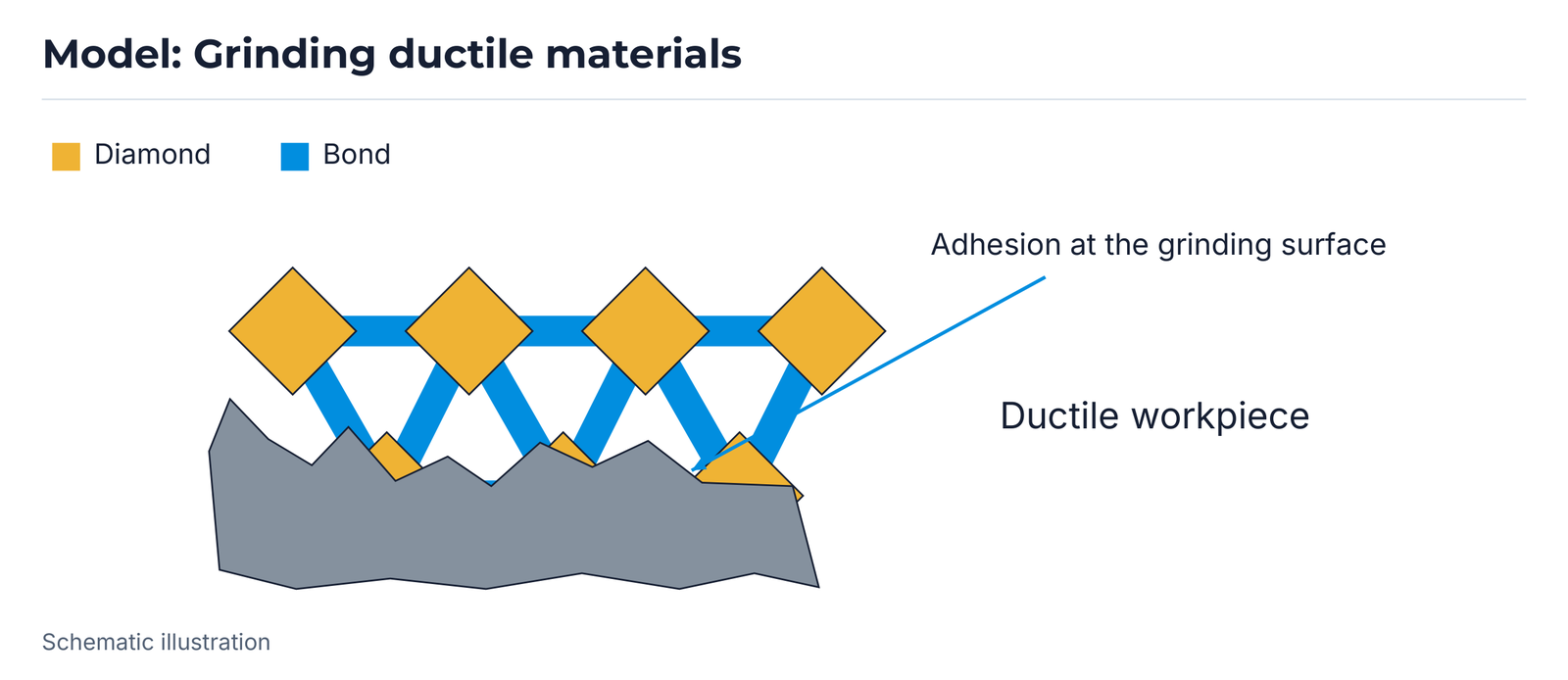
EHWA describes lower bond hardness and reduced bond content as a wheel design approach. These changes can produce thinner bond bridges and encourage renewal of the grinding surface. Adhering material is intended to be removed as the grinding segment renews itself. The required wheel wear is balanced against free-cutting performance, surface requirements and useful wheel life.
Wheel structure for silicon and compound wafers
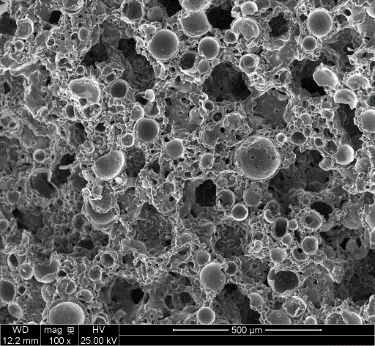
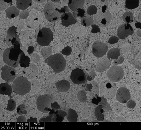
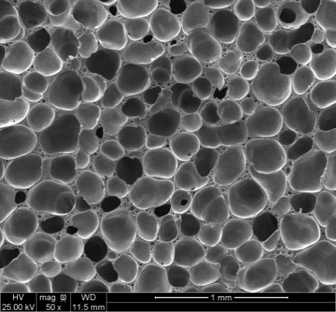
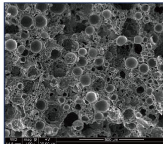
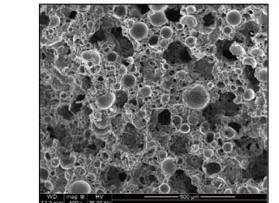
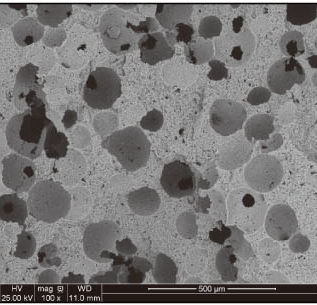
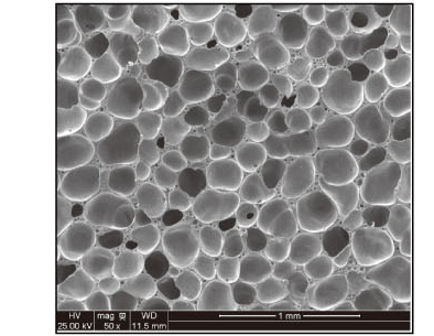
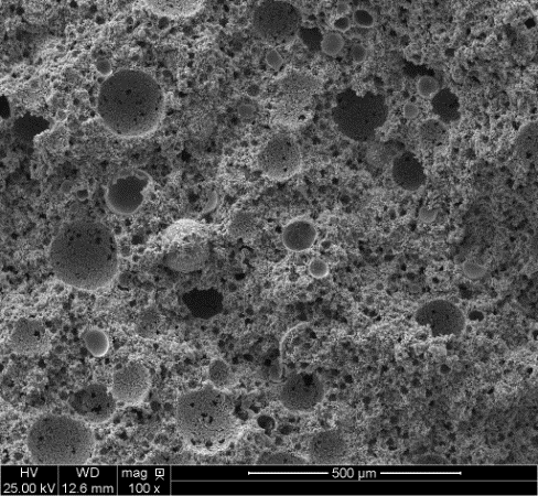
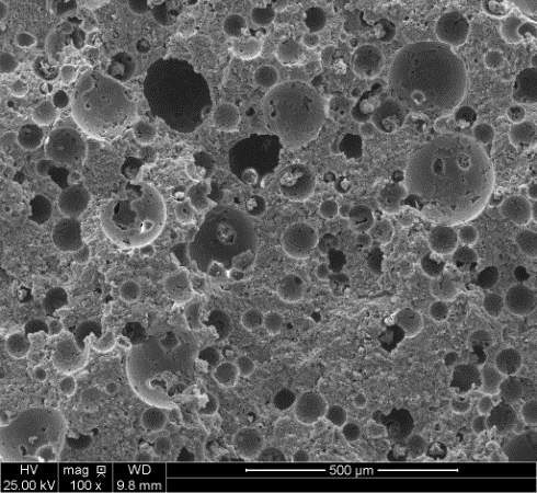
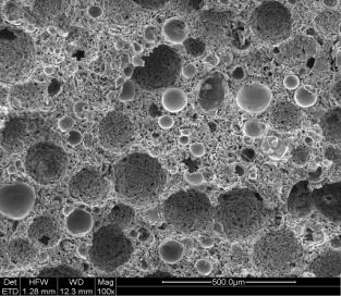
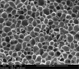
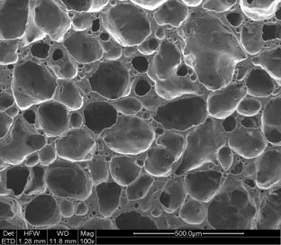
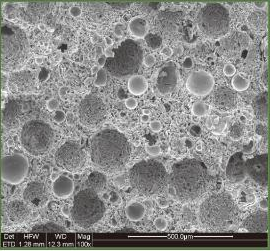
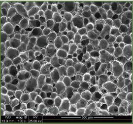
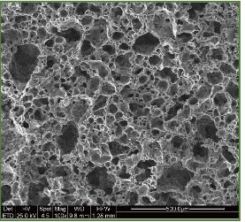
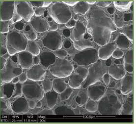
The four images compare grinding segment structures for rough and fine grinding of silicon and compound wafers. Pore structure is one aspect of wheel design. The images show specific designs; they do not establish a single pore size for the entire NANOPOL family.
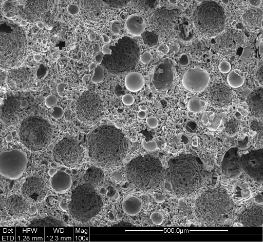

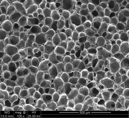
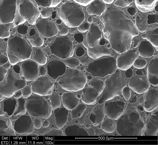
Compound structures and wheel specifications
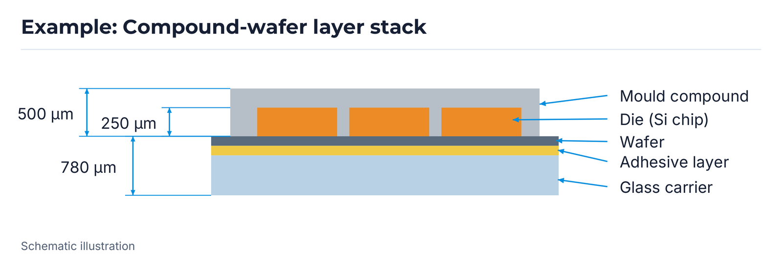
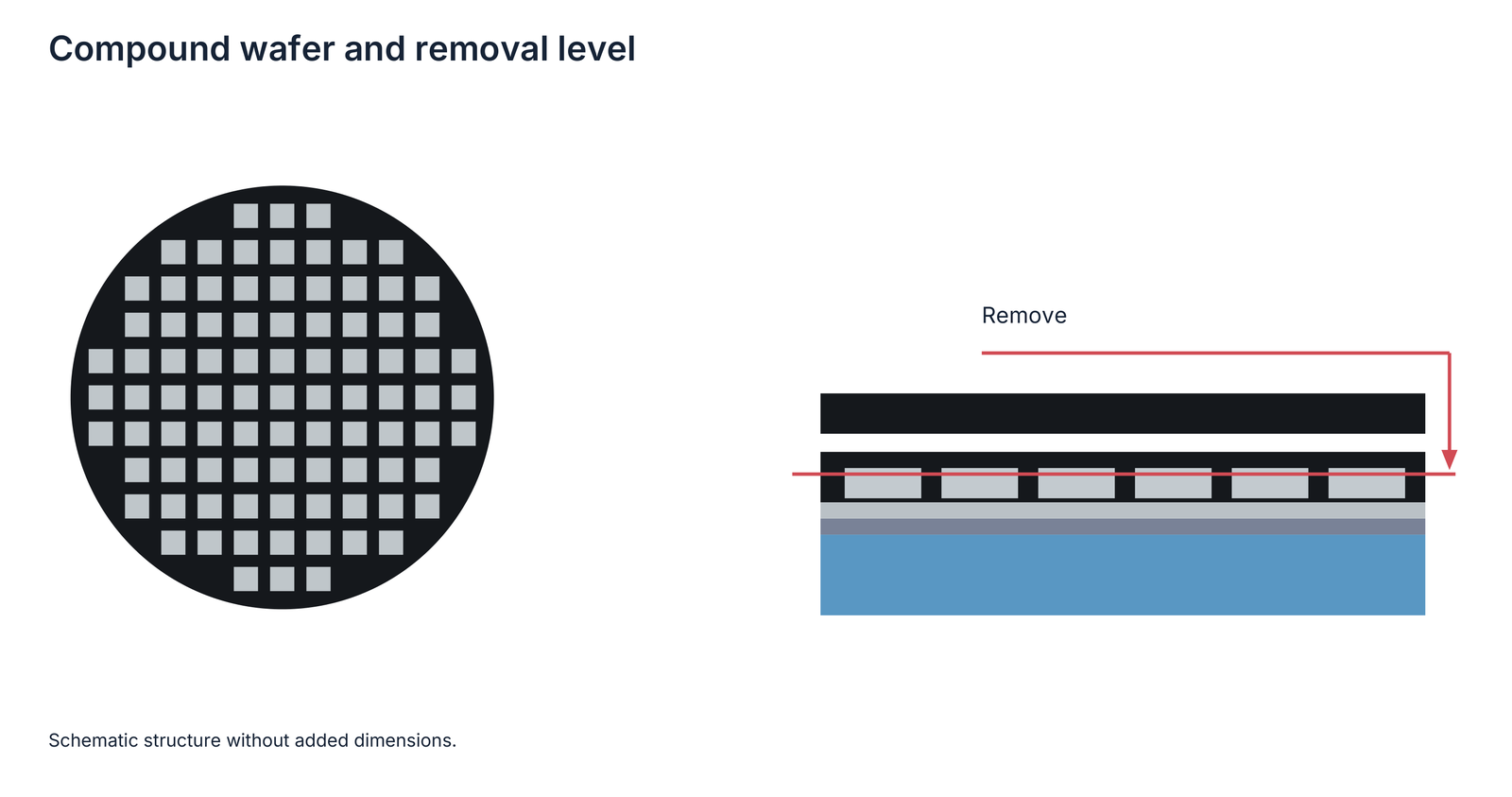
The structure diagrams show mould compound, silicon chips or dies, wafer, adhesive and glass carrier. Another structure includes EMC, silicon chips, tin solder balls and copper vias. The marked removal areas belong to these examples. The dimensions 500 µm, 250 µm and 780 µm in the first layer diagram remain associated with their respective dimension arrows; they are not general wafer dimensions.
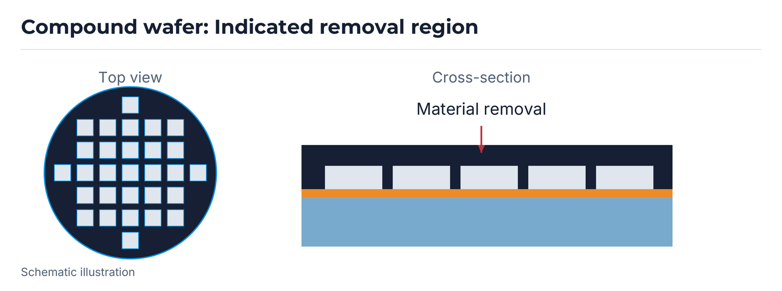

| Material structure | Combination listed in the EHWA document |
|---|---|
| Compound, for example EMC | #325 to #2000 VSP3 or #325 to #2000 VSP5 |
| Compound and silicon chip | Z1 #400 VSP3 + Z2 #4000 to #5500 VK8HS |
| Compound, silicon chip and copper via | Z1 #400 VSP3 + Z2 #4000 to #5500 VK8HS |
| Compound, silicon chip, copper via, polyimide and solder | Design A: Z1 #800 VSP3 + #3000 VK8HS4; design B: Z1 #800 VSP3 + #4000 VSPS10 |
These mappings relate to the illustrated structures. For different proportions of silicon, mould compound or metal, material removal, adhesion, grinding current and surface requirements are considered together again. The complete specification is designed for the actual material composition.
Two wheel concepts for compound wafers
EHWA identifies EMC, polymers, copper and tin as constituents of material structures that can adhere to the grinding segment surface. The document describes two concepts intended to support renewal of that surface.
VSP3 and VK8HS: renew the grinding segment
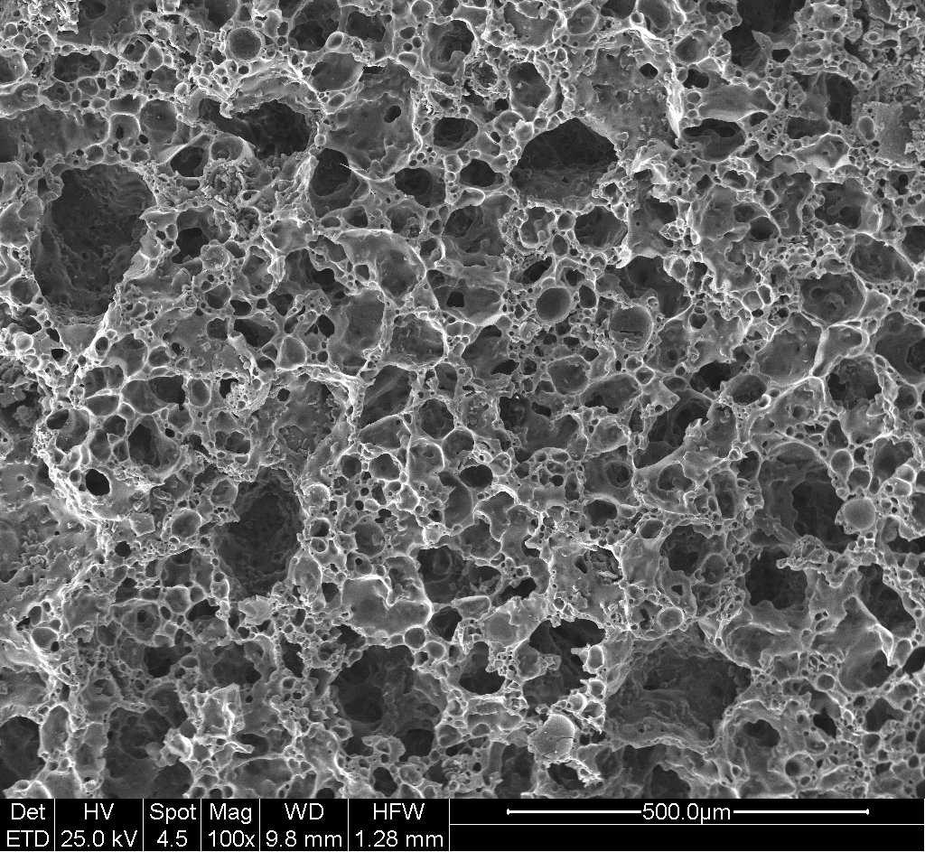
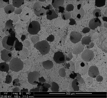
The first concept uses a grinding segment structure that wears more readily. A loaded or smeared grinding surface is intended to renew itself as a result. The illustrated designs are #800-VSP3, #4000-VK8HS and #5000-VK8HS. The three structure images are identified in the document as SEM images at ×100.
VSP5 and VSPS10: thin bond bridges
If loading continues with the first structure, EHWA describes thinner bond bridges between the diamond grains. These bridges are intended to wear or fracture more readily, encouraging renewal of the grinding surface. Adhering constituents are removed from the surface as the wheel wears. The document identifies VSP5 and VSPS10 for this approach and shows #3000-VSPS10 at ×500 and ×2000.
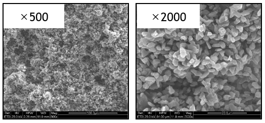

The #3000-VSPS10 example in this structure comparison and #4000 VSPS10 in the material mapping remain separate designs. The series name alone does not establish identical grit size or interchangeability.
Silicon wafers: programme and technology
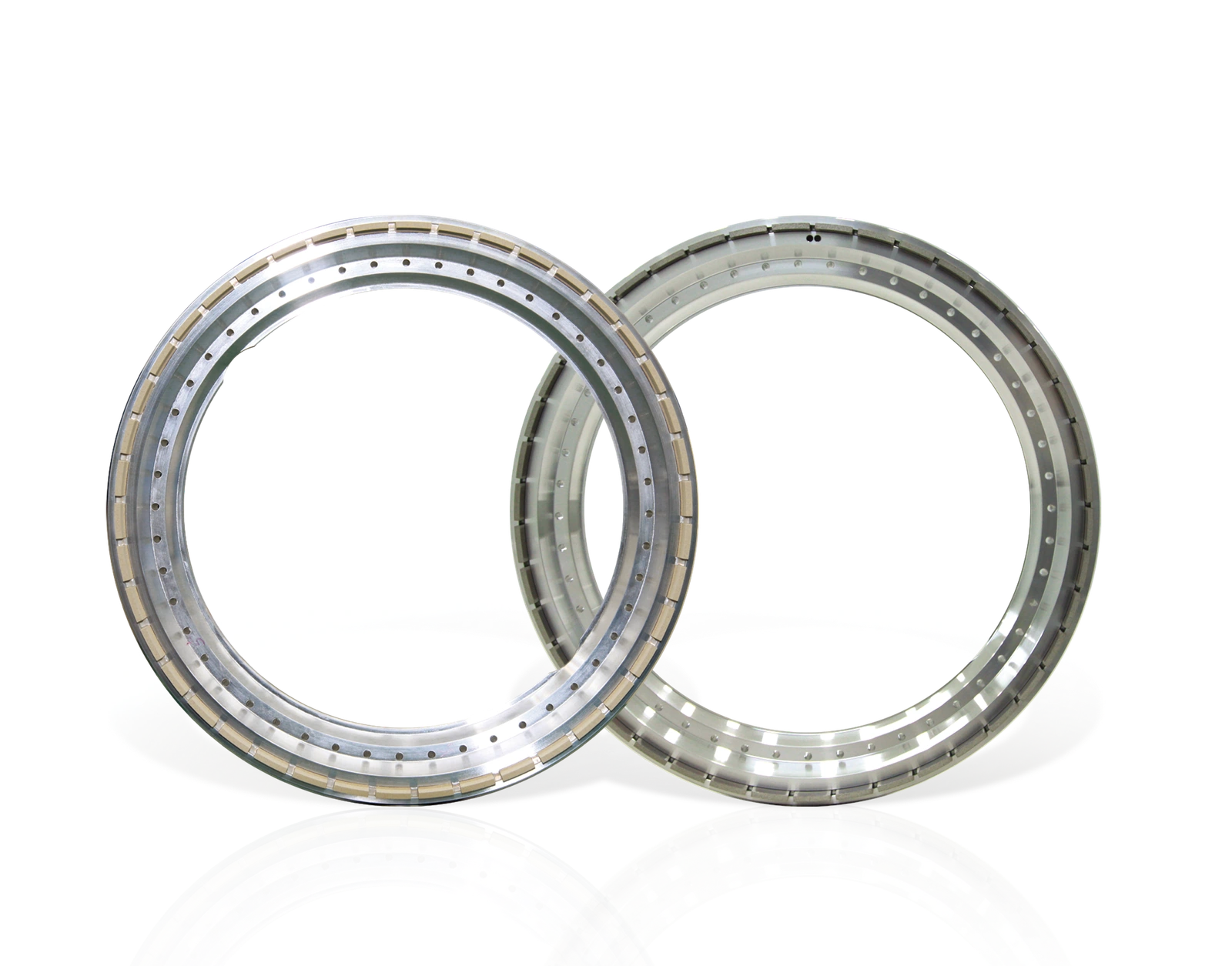
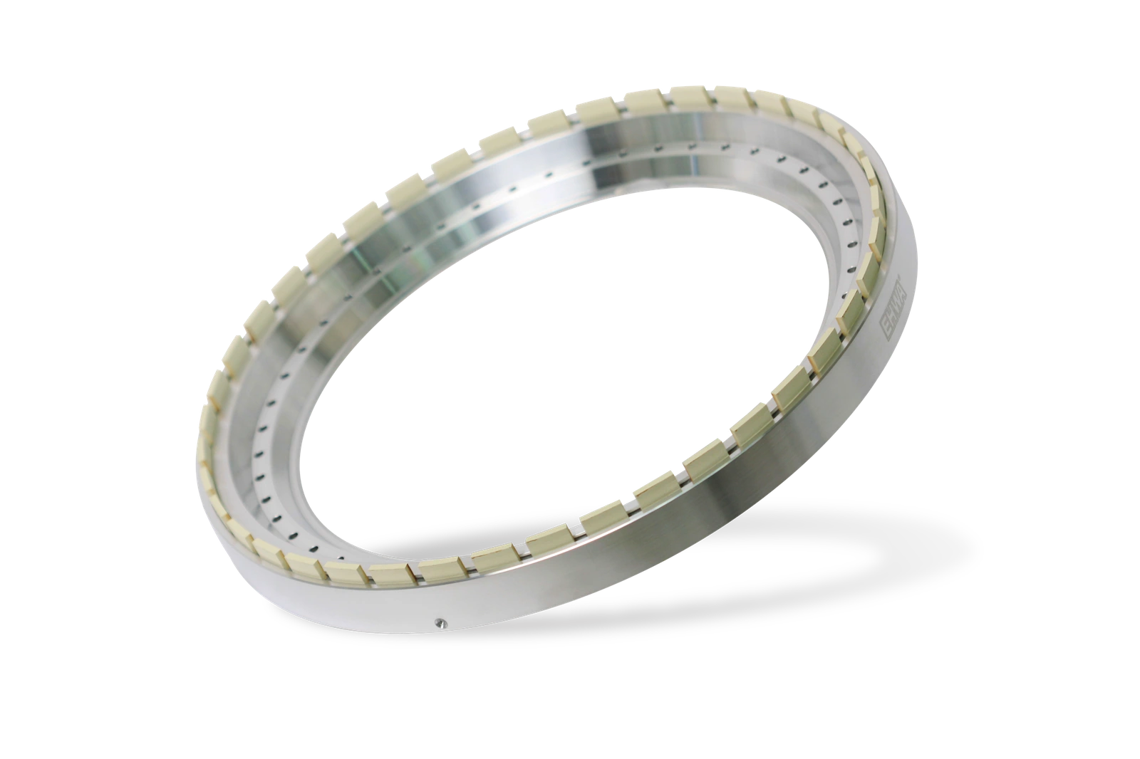
The silicon selection matrix places #400, #600, #800 and #1000 in Z1 rough grinding. The Z2 fine range up to polishing level includes #2000, #3000, #4000, #5000, #6000, #8000, #10000, #20000 and #30000. The following series ranges are highlighted:
| EHWA series | Highlighted grit range |
|---|---|
| VSZT | #400 to #2000 |
| VK8B | #3000 to #5000 |
| VKBT | #3000 to #20000 |
| VNP | #5000 to #30000 |
| VGP | #6000 to #30000 |
For silicon wafers, EHWA describes improved surface roughness and die strength, reduced grinding stress and edge chipping, and consistent diamond distribution. Porosity, pore shape and pore size can be adjusted. The document also identifies ultra-thin silicon wafers down to 17 µm thickness here. Achievable results depend on the complete wheel and process configuration; these features are matched to the required surface and thickness.
Z1: specifications and test example
The Z1 comparison was carried out on a DGP8761. The complete wheel specifications are:
- Design A:
NP-D4-303D3.5W10X-600-VSZT - Design B:
NP-D4-303D3.0W10X-800-VSZT
| Property | Design A: 600-VSZT | Design B: 800-VSZT |
|---|---|---|
| Mean grit size | approximately 20 µm | approximately 16 µm |
| Maximum grit size | approximately 63 µm | approximately 41 µm |
| Reported concentration | 75 | 75 |
| Porosity | approximately 75 vol.% | approximately 75 vol.% |
| Bond | VSZT | VSZT |
| Wheel/chuck speed | 2700/300 min⁻¹ | 3200/300 min⁻¹ |
| Reported feed sequence | 5-3-1 µm/s | 5-3-1 µm/s |
| Grinding current | approximately 13.0 A | approximately 14.0 A |
| Useful wheel life | 15,000 pieces | 12,000 pieces |
Concentration is listed as 75 without a percentage unit in the document; porosity is explicitly expressed as volume percent. The feed sequence is reproduced unchanged. The different wheel speeds belong to the respective test designs and remain part of the comparison.

Damage layer after Z1 grinding
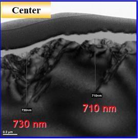
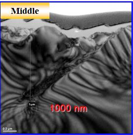
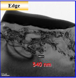
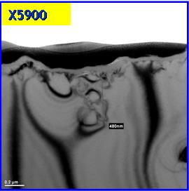
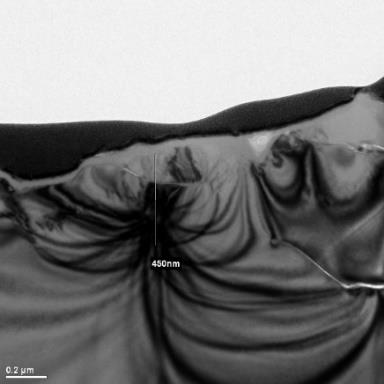
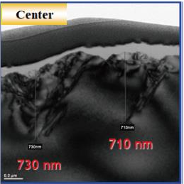
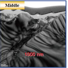
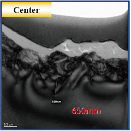
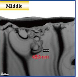
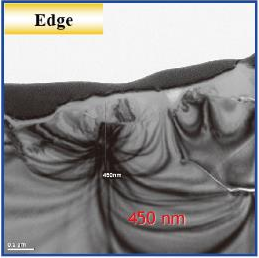
The images compare the wheels identified in the document as Resin #325 and Vitrified #600. Centre, middle and edge remain separate measurement positions. Two values are marked at the centre in the resin example.
| Wheel in the image comparison | Centre | Middle | Edge |
|---|---|---|---|
| Resin #325 | 730 nm and 710 nm | 1000 nm | 540 nm |
| Vitrified #600 | 650 nm | 480 nm | 450 nm |
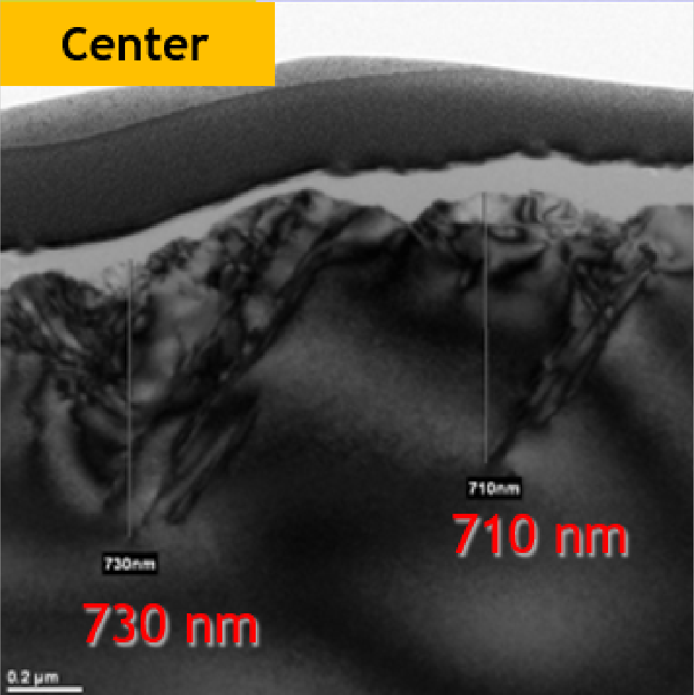
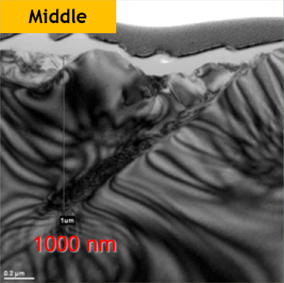
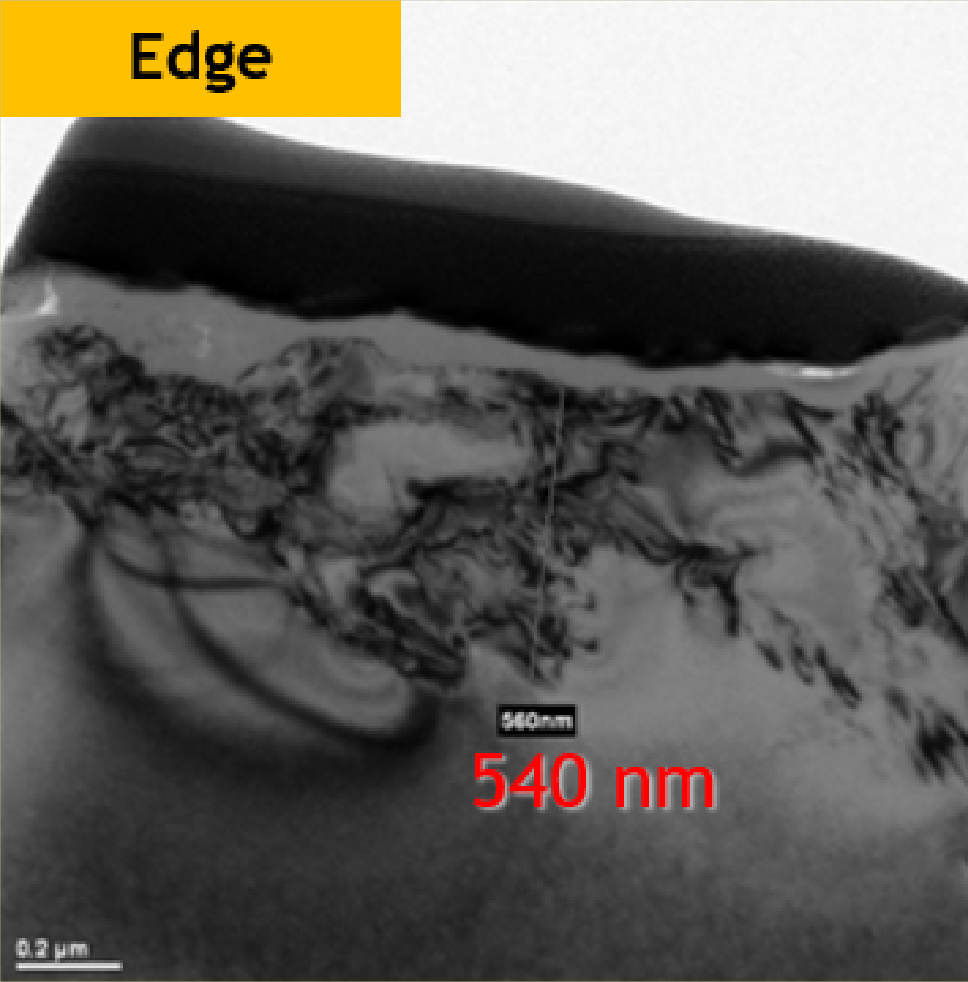
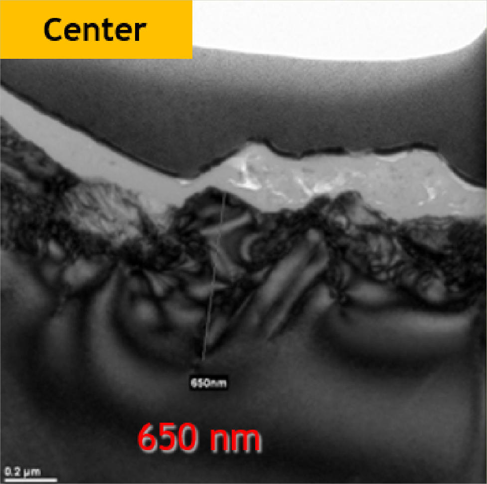
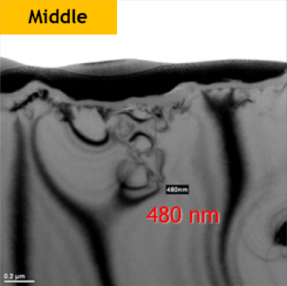
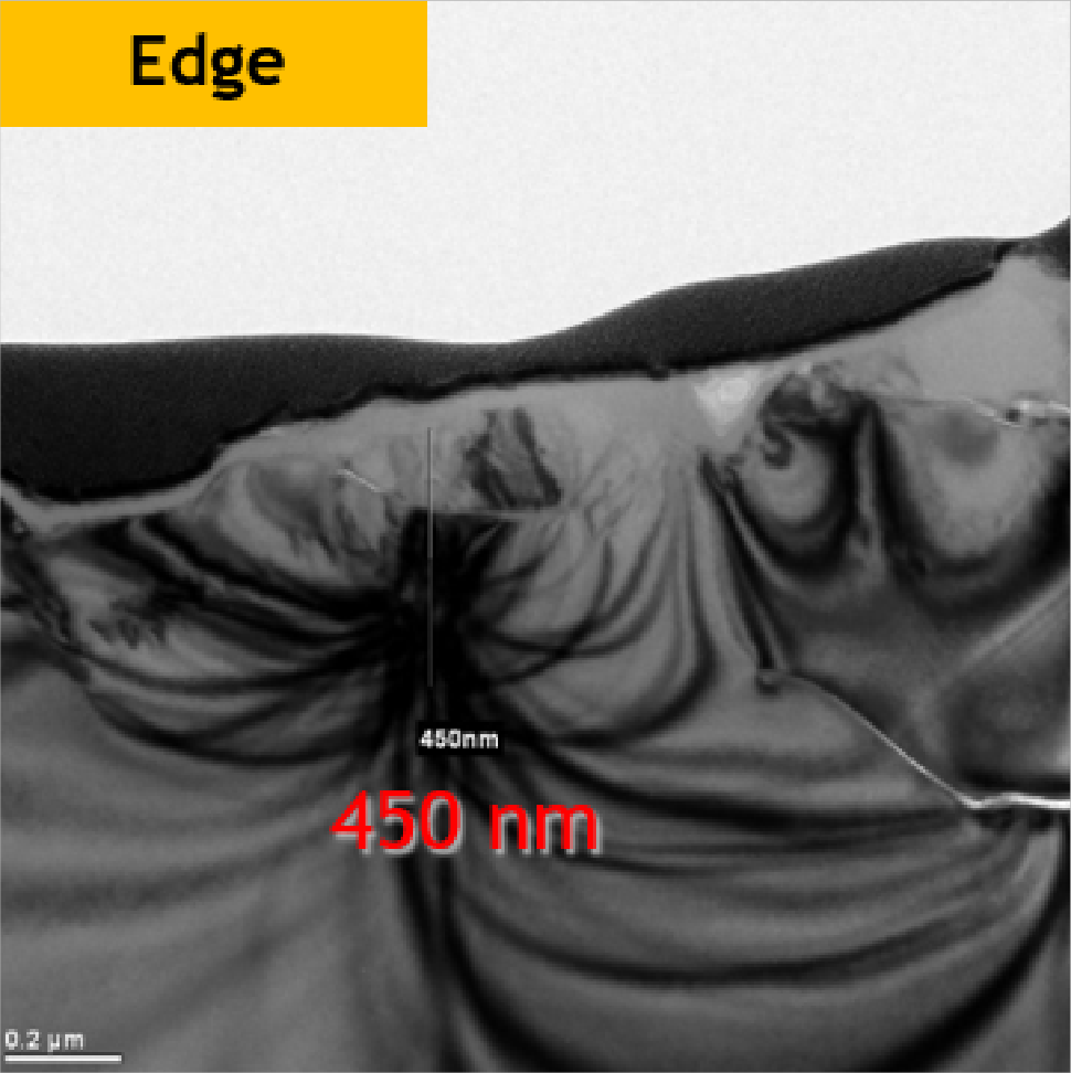
The values belong to the illustrated cross-section images. They describe this image comparison and do not establish a general damage depth for all resin-bond or vitrified-bond wheels. The process conditions for the two image sets are not fully documented in the source.
Z2: specifications, roughness and useful wheel life
The Z2 comparison also identifies the DGP8761. Roughness was measured using a Wyco Veeco NT9100. The complete specifications are:
- Design C:
NP-D4-303D3.5W10X-5000-VKBT25 - Design D:
NP-D4-303D3.0W7X-8000M-VNPSSR
| Property | Design C: 5000-VKBT25 | Design D: 8000M-VNPSSR |
|---|---|---|
| Mean grit size | approximately 2.0 µm | approximately 0.55 µm |
| Maximum grit size | ≤ 5.5 µm | ≤ 1.2 µm |
| Feed rate | 0.6 µm/s | 0.2 µm/s |
| Grinding current | 13.5 A | 15.5 A |
| Useful wheel life | 23,000 pieces | 4,500 pieces |
| Ra roughness | approximately 4.8 nm | approximately 1.3 nm |
| Rmax roughness | approximately 56 nm | approximately 15 nm |
The wheels differ in specification and feed rate. The test illustrates the relationship between surface requirements, processing conditions and useful wheel life. It is not a wheel-life comparison under identical conditions. Selection considers required roughness, available processing time and existing grinding stages together.
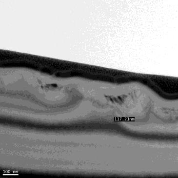
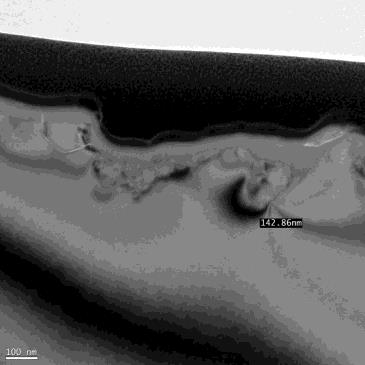
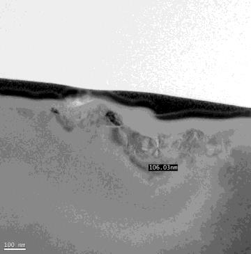
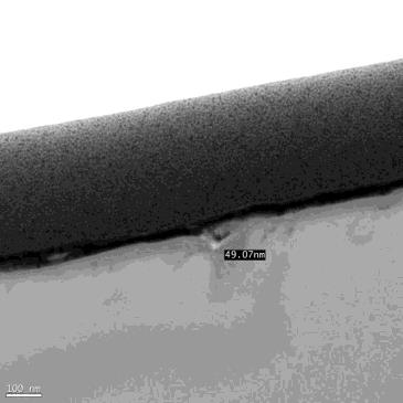
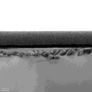
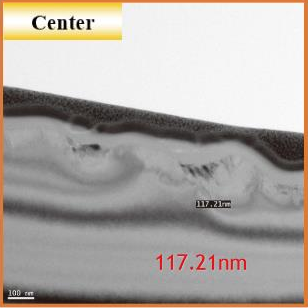
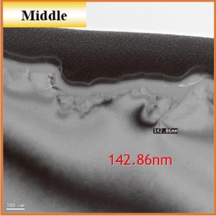
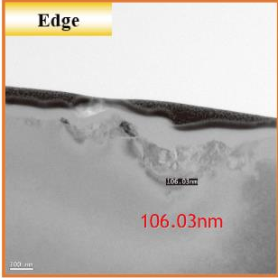
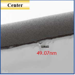
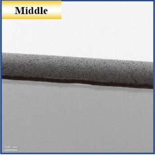
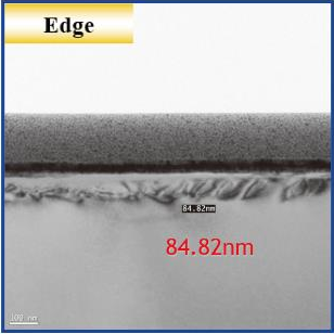
Damage layer with the #5000 and #8000 designs
The following images show vitrified-bond designs labelled Vitrified #5000 and Vitrified #8000. Centre, middle and edge remain individually identified measurement positions.
| Wheel in the image comparison | Centre | Middle | Edge |
|---|---|---|---|
| Vitrified #5000 | 117.21 nm | 142.86 nm | 106.03 nm |
| Vitrified #8000 | 49.07 nm | no numerical value reported | 84.82 nm |
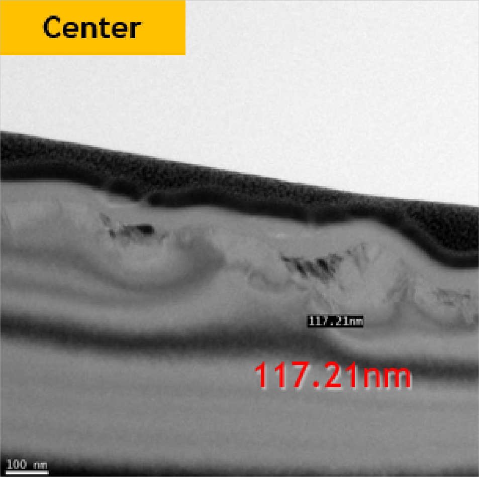
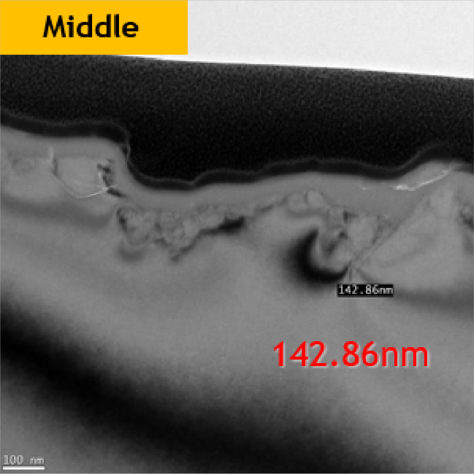
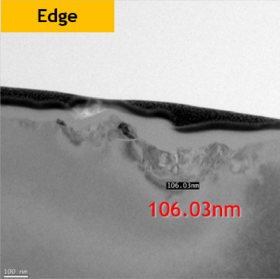
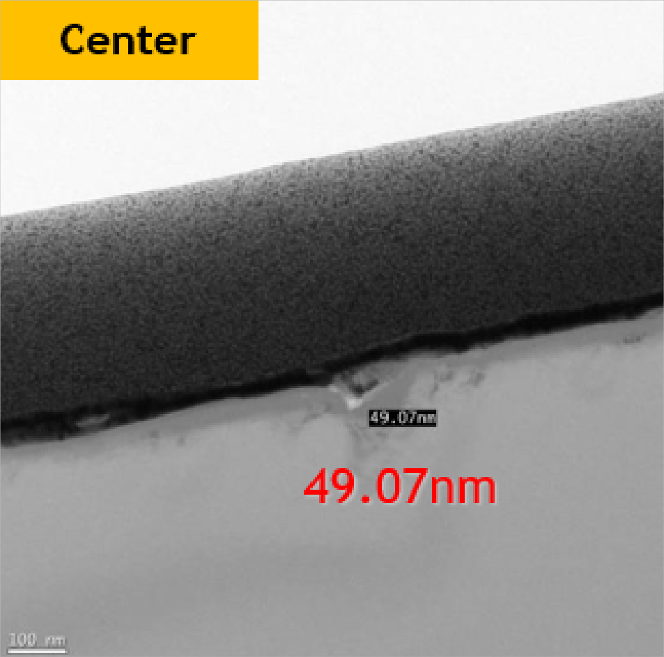

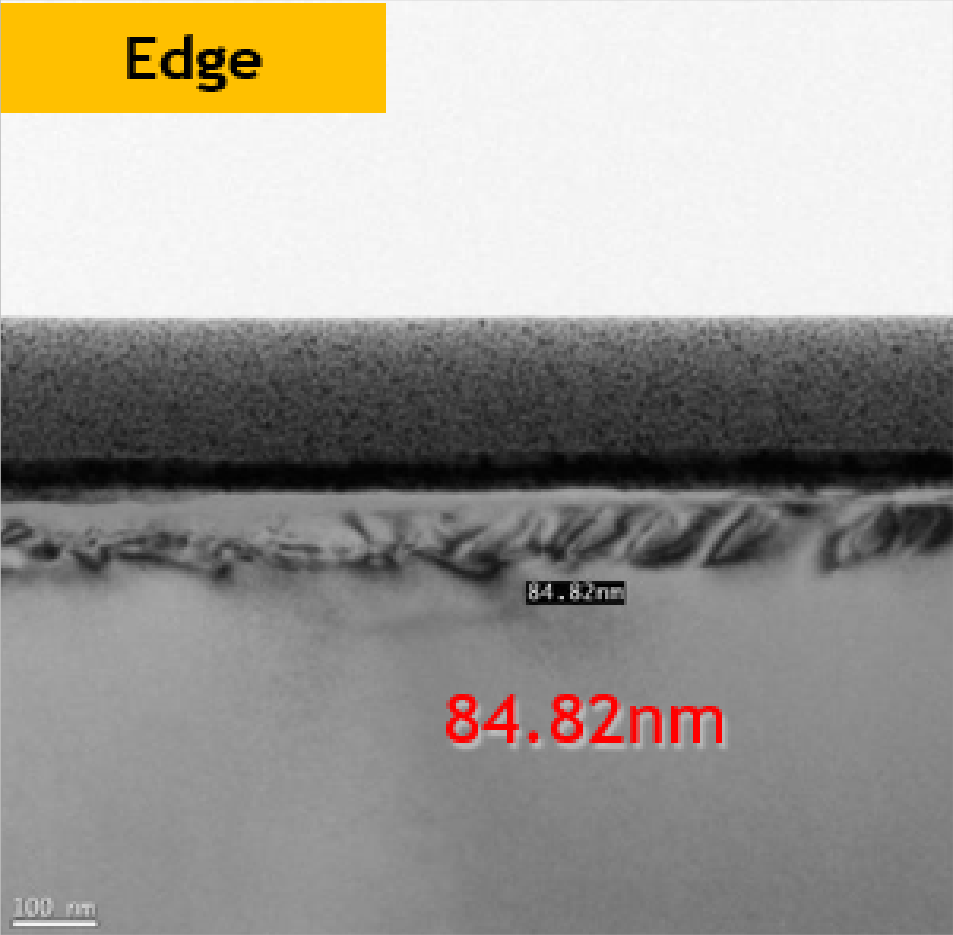
No measured value is added for the middle image of the #8000 design. The image labels #5000 and #8000 are not equated with the complete specifications of the preceding test without additional evidence. The values describe the illustrated images; they do not establish a universally guaranteed damage depth.
NANOPOL selection matrix for multiple materials
Documents Q221 and Q233 add a joint selection matrix to the material-specific programmes. It distinguishes silicon from SiC, sapphire, LT/LN, glass and EMC. LT/LN retains the combined material group used in the source; EMC means epoxy moulding compound. The matrix lists #400, #600, #800 and #1000 under Z1, and #2000, #3000, #4000, #5000, #6000, #8000, #10000, #20000 and #30000 under Z2. The original colour coding is represented here by a material column.
| Series | Material group | Marked range |
|---|---|---|
| VSZT | Si | #400–#3000 |
| VNP | SiC / Glass | #1000–#2000 |
| VSBT | Sapphire / Glass | #800–#3000 |
| VSP | LT/LN / Sapphire / EMC | #400–#5000 |
| VSPS | EMC | #2000–#6000 |
| VK8B | Si | #4000–#6000 |
| VK8B | SiC / EMC | #5000–#6000 |
| VK8HS | EMC | #3000–#6000 |
| VNP | Si | #6000–#30000 |
| VNP | SiC | #6000–#8000 |
| VKBT25 | Si | #5000–#20000 |
Independent silicon selection matrix in the combined sheet
Combined sheet Q272 shows an independent silicon programme using the same grit list. Its ranges are kept separate from the main NANOPOL programme. The matrix supports selection between coarser removal and fine surface finishing; it does not approve every intermediate grit for every machine.
| Series | Q272: marked range |
|---|---|
| VSZT | #400–#3000 |
| VK8B | #4000–#6000 |
| VKBT | #4000–#20000 |
| VNP | #6000–#30000 |
| VGP | #8000–#30000 |
The Z1 and Z2 test tables in the combined sheet agree with the complete main-programme tables: Z1 uses NP-D4-303D3.5W10X-600-VSZT and NP-D4-303D3.0W10X-800-VSZT; Z2 uses NP-D4-303D3.5W10X-5000-VKBT25 and NP-D4-303D3.0W7X-8000M-VNPSSR. The machine is specified as DGP8761. The individual images from the combined sheet are additionally retained.
Z1: vitrified and resin-bonded versions compared
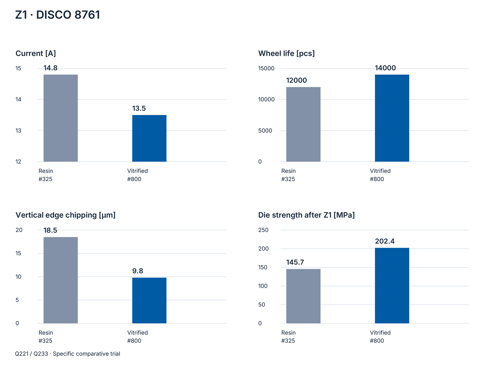
On the DISCO 8761, Q221 compares resin #325 with vitrified #800. Q233 repeats the four results. In this test, the vitrified version shows lower current, greater wheel life, less vertical edge chipping and higher die strength after Z1. These values belong to this comparison; general tool selection also considers feed rate, mounting and the remaining process chain.
| Measured quantity | Resin #325 | Vitrified #800 |
|---|---|---|
| Grinding current [A] | 14.8 | 13.5 |
| Wheel life [pcs] | 12000 | 14000 |
| Vertical edge chipping [µm] | 18.5 | 9.8 |
| Die strength, Z1 only [MPa] | 145.7 | 202.4 |
Damage layer: image designations in the comparative editions
Comparative edition Q221 shows damage depths at the centre, middle and edge. The upper row is labelled Resin #325. The lower row is labelled “Vitri #8000” there; Q284 uses “Vitrified #600” for the corresponding numerical series. Q233 repeats the measurement images without the same complete tool designation. The source designations are retained separately rather than harmonised into one specification.


Silicon fine grinding: additional specifications and test data
Documents Q221 and Q233 contain a further Z2 comparison on the DISCO 8761. Segment height is specified as 7 mm. Grit data and roughness values agree between the two documents, while Q233 uses shorter specification codes. The full Q221 codes are therefore explicitly paired with the Q233 designations. This comparison is retained alongside the main programme: current, feed and wheel life differ from the Q284/Q272 test.
Surface measurement used a Wyko Veeco NT9100. The differences in feed and wheel life help relate the required surface target to economical processing time.
| Characteristic | #5000 version | #8000M version |
|---|---|---|
| Q221 code | #5000-VKBT25M3-P12 | #8000M-VNP-HBF |
| Q233 code | #5000-VKBT25M3 | #8000M-VNP |
| Mean grit size [µm] | ~2.0 | ~0.55 |
| Maximum grit size [µm] | ≤5.5 | ≤1.2 |
| Current / feed | 13.5 A / 0.6 µm/s | 12.7 A / 0.2 µm/s |
| Wheel life [pcs] | 17000 | 3000 |
| Ra [nm] | ~4.8 | ~1.3 |
| Rmax [nm] | ~56 | ~15 |
The additional damage images in Q221 show #5000 at 117.21 / 142.86 / 106.03 nm and #8000 at 49.07 nm in the centre and 84.82 nm at the edge. No measured number is added for the middle #8000 image. Q233 and the main programme also show this numerical series; the original images retain their scales and measurement markings.



SiC: grit, wear and surface finish
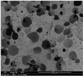
Q221 adds an SiC comparison to the silicon programme. Different grinding amounts are specified for the two versions. Reported wheel wear therefore describes two specific processing conditions. The very fine version has markedly smaller grit and a finer measured surface. Surface measurement used a Wyko Veeco NT9100; each Rmax value retains its original unit.
| Characteristic | #2000 version | #8000M2 version |
|---|---|---|
| Specification | #2000-VNP8-GC | #8000M2-VNP-PSR |
| Mean grit size [µm] | ~7.0 | ~0.55 |
| Maximum grit size [µm] | ≤26.0 | ≤1.2 |
| Wheel wear [µm] | 20 | 15 |
| Grinding amount [µm] | 100 | 20 |
| Ra [nm] | ~18 | ~1.5 |
| Rmax | ~1.3 µm | ~14 nm |
Additional compound specifications
The compound tables in Q012/Q026 and Q221/Q233 supplement the full specifications in the main programme. The material structures are distinguished individually: pure moulding compound; compound with silicon chips; additionally copper vias; and the complex structure incorporating polyimide and solder. The older selection lists VSPBT7 as a second alternative for the complex structure. Q221/Q233 list VSPS10 only at that position. These variants are expressly retained rather than transferring their codes into the later main programme.
The drawings explain silicon, EMC, copper and solder, plus a polyimide layer. The simpler earlier drawing has no individually designated copper or solder markers. Appropriate bond and pore structures support particle removal and the processing of different material constituents on the same grinding surface.
| Material structure | Q012 / Q026 | Q221 / Q233 |
|---|---|---|
| Pure EMC | #800–#2000 VSP3 / #800–#2000 VSP5 | same |
| EMC + Si chip | Z1 #800 VSP3 + Z2 #5000 VK8HS / #5000 VK8B | same |
| EMC + Si chip + Cu via | Z1 #800 VSP3 + Z2 #5000 VK8HS / #5000 VK8B | same |
| EMC + Si chip + Cu via + Polyimide + Solder | Z1 #800 VSP3 + #3000 VSPS10 / #3000 VSPBT7 | Z1 #800 VSP3 + #3000 VSPS10 |
The source headings also list Fingerprint Strip and Compound Molded Wafer for TSV/Fan-Out as application designations. Micrographs retain each original silicon/compound and rough/fine assignment.


Early Z1 and combined Z1+Z2 comparison diagrams
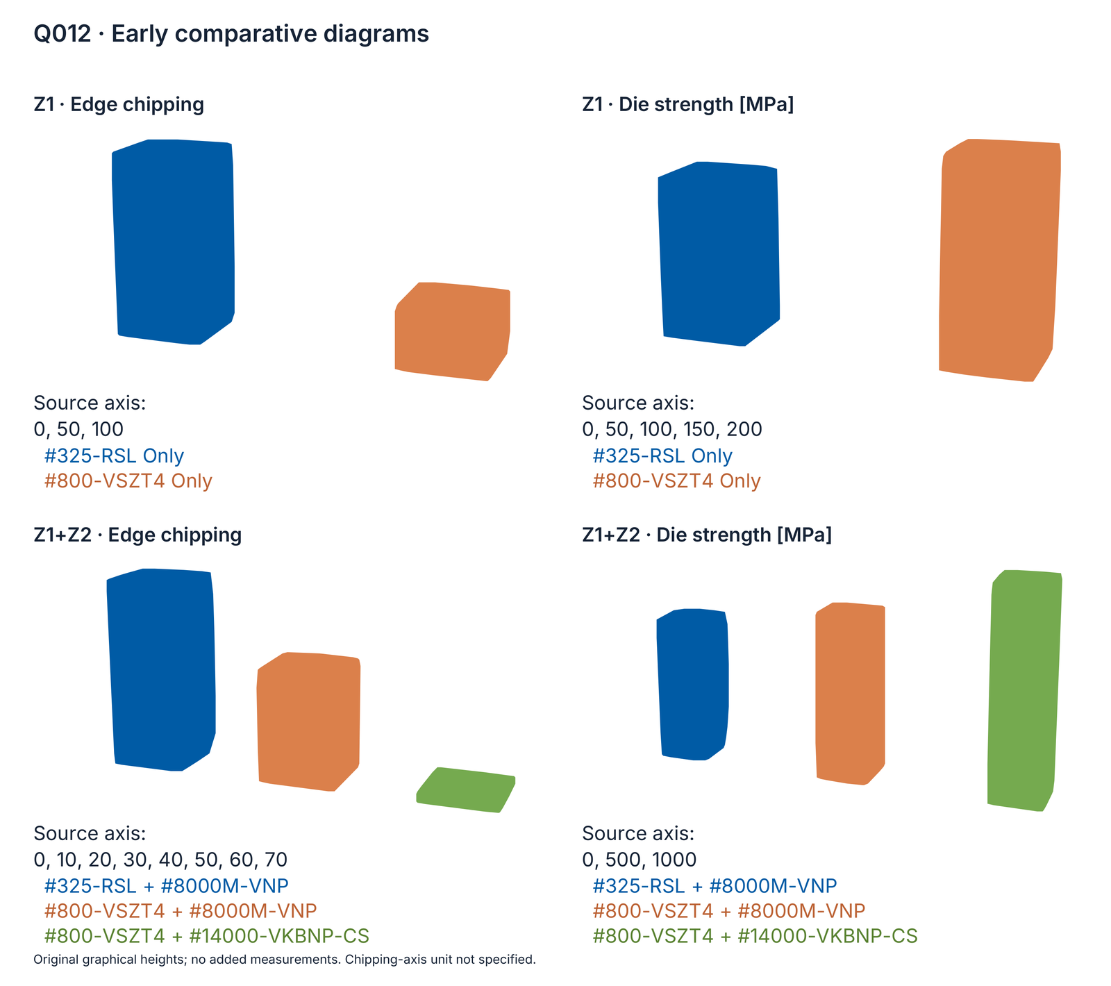
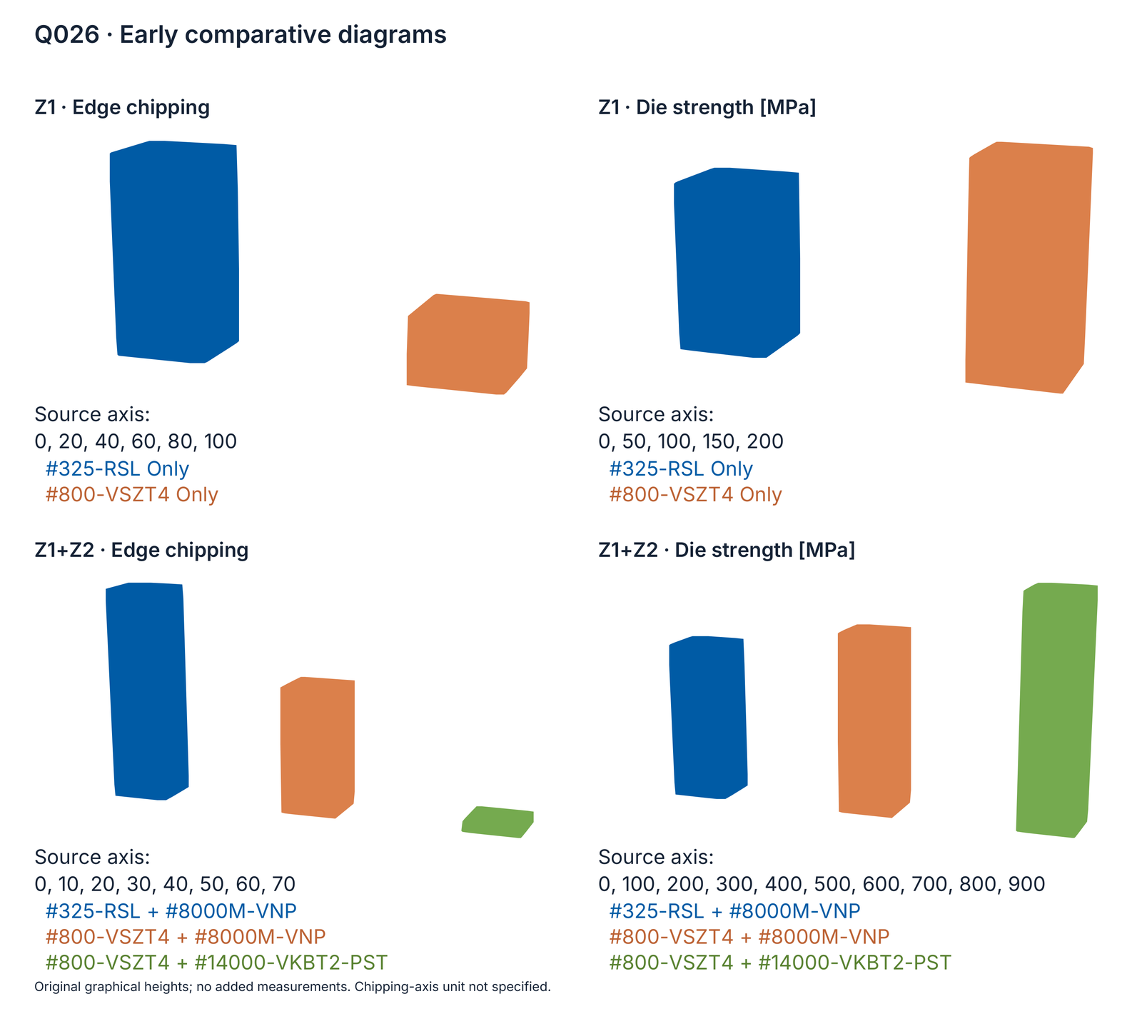
The two editions printed in January 2017 compare edge chipping and die strength after Z1 and after combined Z1+Z2. They show the change from #325-RSL to #800-VSZT4 and different fine-grinding stages. Individual measured numbers are not printed on the bars; their relative heights are therefore retained as graphical comparisons. The strength axis is labelled MPa. No unit is specified for the edge-chipping axis.
The two Z1 versions are #325-RSL Only and #800-VSZT4 Only. The Z1+Z2 combinations are #325-RSL + #8000M-VNP, #800-VSZT4 + #8000M-VNP, and the tool-specific third combination. In Q012 this is #800-VSZT4 + #14000-VKBNP-CS; in Q026 it is #800-VSZT4 + #14000-VKBT2-PST. These codes are not equated with later trials. The new diagrams retain the original axis scales and graphical heights without deriving additional numerical measurements.
Sapphire and hard materials: programme variants
The sapphire documents describe high stock-removal performance and long wheel life in metal-bonded rough grinding, and fine surfaces in vitrified fine grinding. The programme targets sapphire, SiC, glass and other hard materials such as zirconia. Q030 additionally names brittle materials. Tool construction and processing parameters can be adapted to different machines and grinding methods.
Both documents carry a January 2017 print date. Their programme tables nevertheless differ in series, diameters, segment heights and grit ranges. D denotes diameter, W segment width and X segment height. Slant and Segment retain the source form designations.
| Source | Stage | Series | D [mm] | W [mm] | X [mm] | Grit | Form |
|---|---|---|---|---|---|---|---|
| Q003 | Rough | MX / MS Series | 200–300 | 3–5 | 3–10 | #170–#500 | Slant / Segment |
| Q003 | Fine | MS / VSP / VSBT Series | 200–300 | 3–5 | 3–10 | #600–#5000 | Slant / Segment |
| Q030 | Rough | MX Series | 250 / 300 / 380 | 3–5 | 5–10 | #170–#600 | Slant / Segment |
| Q030 | Fine | MF / VSP Series | 200 / 250 / 300 | 3–5 | 5–10 | #800–#1500 | Slant / Segment |

Eight sapphire and ceramic application examples
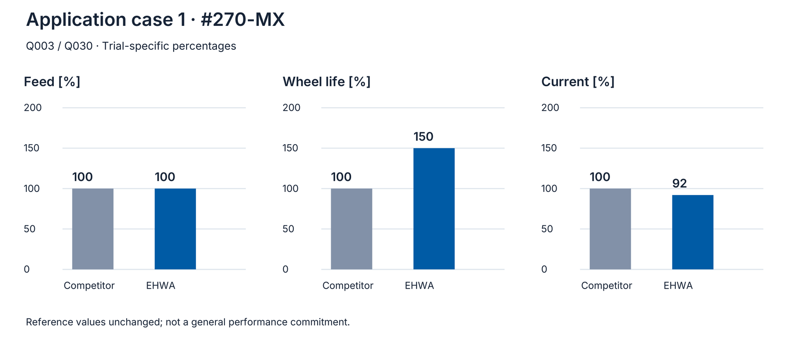
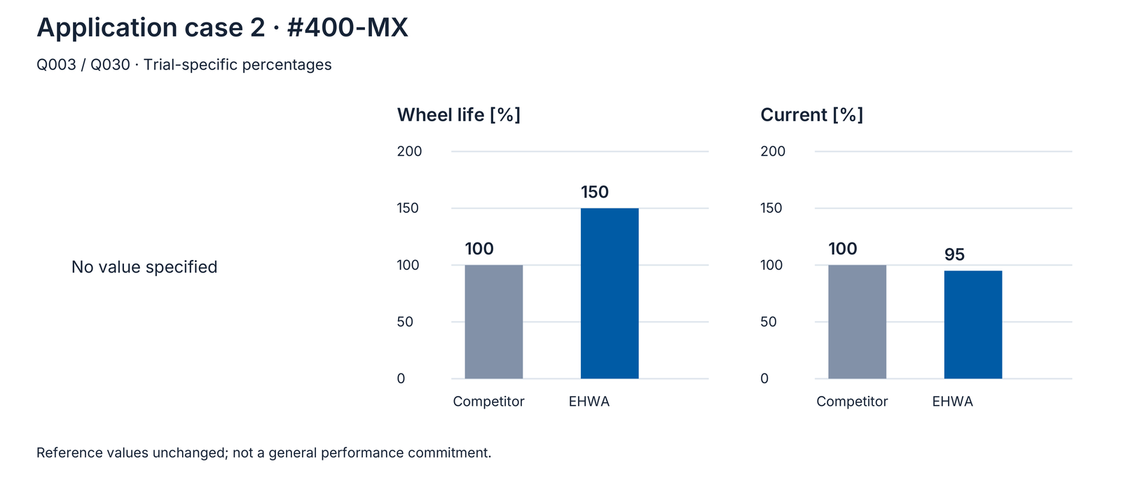
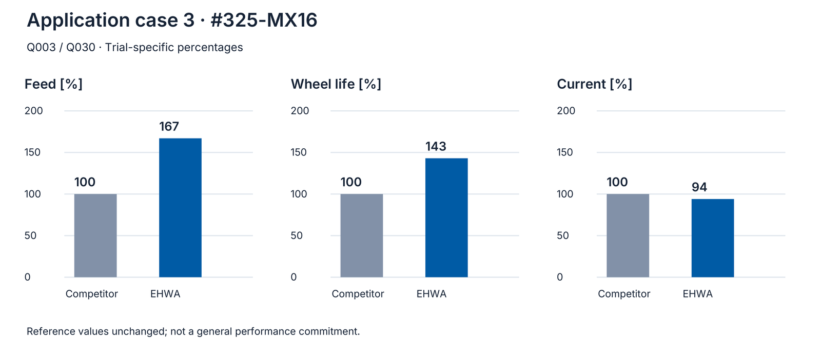
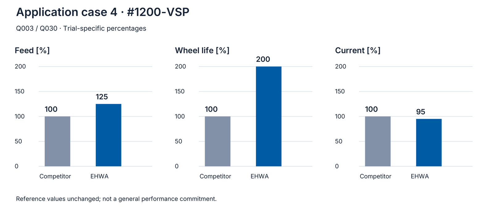
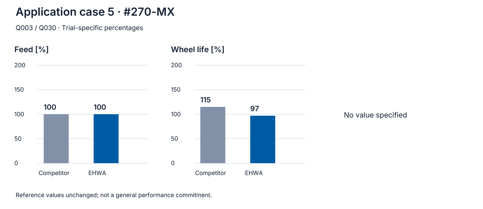
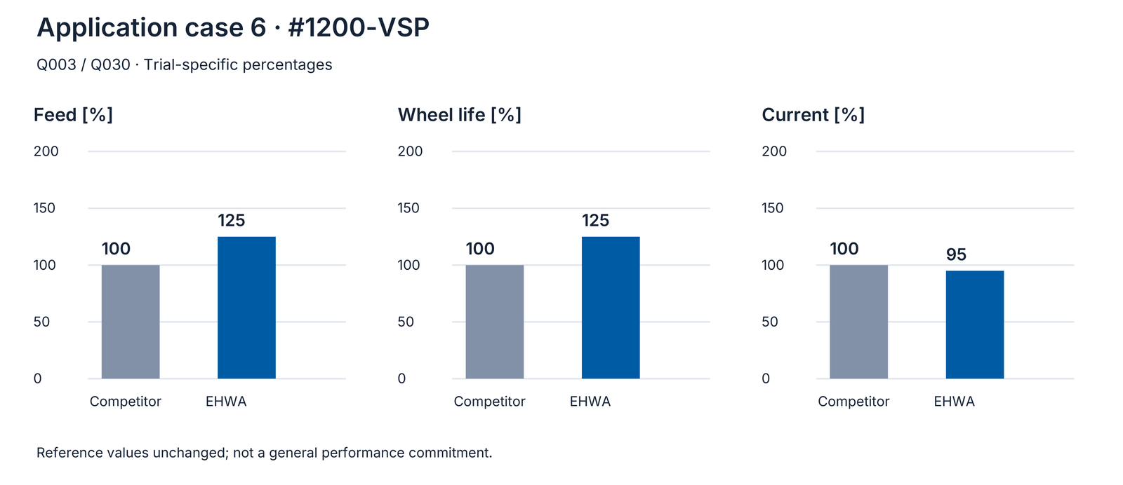
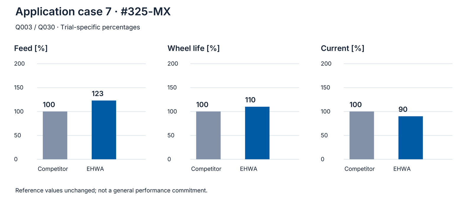
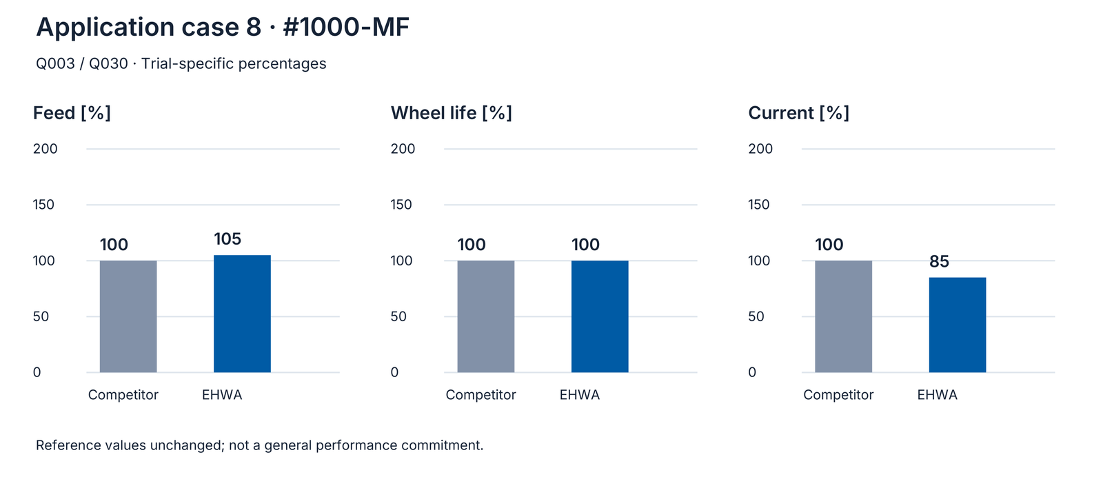
Q003 and Q030 contain the same eight application cases and printed comparative numbers. They are presented once in full. The sources distinguish wafer size, WAX or TAPE mounting, rough/fine tools and fully automatic machining. Percentages are relative values within the particular trial rather than general performance guarantees.
Numbers in the table are always ordered competitor / EHWA. In the 6-inch rough-grinding case, wheel life is expressly 115 / 97; this independent reference presentation is not normalised to 100. In the 8-inch fine-grinding case, both life bars carry the printed value 100 despite their different original graphical heights. The new edition uses the printed numbers.
| Case | Workpiece / mounting | Tool | Feed [%] | Wheel life [%] | Current [%] |
|---|---|---|---|---|---|
| 1 | 2–4" Sapphire / WAX | #270-MX | 100 / 100 | 100 / 150 | 100 / 92 |
| 2 | 2–4" Sapphire / WAX | #400-MX | — | 100 / 150 | 100 / 95 |
| 3 | 4" Sapphire / WAX / fully automatic | #325-MX16 | 100 / 167 | 100 / 143 | 100 / 94 |
| 4 | 4" Sapphire / WAX / fully automatic | #1200-VSP | 100 / 125 | 100 / 200 | 100 / 95 |
| 5 | 6" Sapphire / TAPE / fully automatic | #270-MX | 100 / 100 | 115 / 97 | — |
| 6 | 6" Sapphire / TAPE / fully automatic | #1200-VSP | 100 / 125 | 100 / 125 | 100 / 95 |
| 7 | 8" Ceramic / TAPE / fully automatic | #325-MX | 100 / 123 | 100 / 110 | 100 / 90 |
| 8 | 8" Ceramic / TAPE / fully automatic | #1000-MF | 100 / 105 | 100 / 100 | 100 / 85 |
6-inch sapphire: surface and wafer images
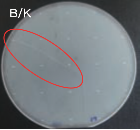
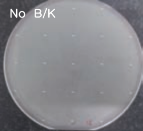
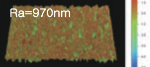
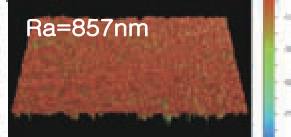
For rough grinding with #270-MX on 6-inch sapphire using TAPE mounting, the originals show wafer photographs marked B/K for the competitor and No B/K for EHWA. These abbreviations are retained as source designations. The associated surface images carry Ra 970 nm for the competitor and Ra 857 nm for EHWA. These two images supplement the specific trial rather than describing every sapphire tool.
Resin-bonded and vitrified back-grinding versions
The document printed in December 2018 distinguishes two Z1 concepts. Vitrified tools #400–#800 enable higher feed and consequently higher units per hour; low, consistent current supports long wheel life. Resin-bonded tools #325–#600 target reduced edge chipping and damage on thin wafers, with good grinding performance and useful tool life.
For Z2, EHWA describes resin #2000–#4000 with low, stable current and longer life than the comparative tool. Finer #3000–#4000 versions target improved roughness and fewer grinding marks. D, W and X are defined as diameter, width and depth. Q101 does not print a unit beside the dimension list below.
The independent selection lists are not row-by-row specification combinations. Machine abbreviations, grits and bonds are therefore listed separately.
| Selection list | Q101 data |
|---|---|
| D | Ø200–Ø204 / Ø250 / Ø300–Ø304 |
| W | 2–4 |
| X | 5–7 |
| Bond type | Resin BG01 / Vitrified BG02 |
| Machine / SK type | DISCO D / OKAMOTO O / TSK T |
| Mesh size | #270 / #325 / #400 / #600 / #800 / #1200 / #1500 / #2000 / #3000 / #4000 |
| Bond name | VA / VCL / RB / RS / REC / RDC / SWB / SWA / SWC / SWD / SWE |
Back grinding: DISCO and TSK trials
The Z1 trials compare EHWA porous resin bond RSL with a porous competitor bond. Z2 compares EHWA wear-resistant porous resin bond SWD. The tables retain each comparative grit and the machine-specific wheel-life values. The source designates the current figures as maximum grinding current at normal feed. K here means one thousand wafers per wheel.
The edge images marked X40 show a remaining wafer thickness of 90 µm after rough grinding with #600 RSL and 50 µm after fine grinding with #3000 SWDL. The image designation SWDL is retained alongside table bond SWD.
Z1
| Characteristic | EHWA / DISCO | EHWA / TSK | Competitor / DISCO | Competitor / TSK |
|---|---|---|---|---|
| Bond / grit | RSL / #400–#600 | RSL / #400–#600 | Porous resin / #320 | Porous resin / #320 |
| Machine | DISCO 8760 | TSK PG300 | DISCO 8760 | TSK PG300 |
| Current [A] | ~12–13 | ~9–10 | ~13–14 | ~10–11 |
| Wheel life [wafers/wheel] | ~18K | ~12K | ~13K | ~10K |
| Rmax [µm] | ~3–4 | ~3–4 | ~4–5 | ~4–5 |
Z2
| Characteristic | EHWA / DISCO | EHWA / TSK | Competitor / DISCO | Competitor / TSK |
|---|---|---|---|---|
| Bond / grit | SWD / #2000–#3000 | SWD / #2000–#3000 | Porous resin / #2000 | Porous resin / #2000 |
| Machine | DISCO 8760 | TSK PG300 | DISCO 8760 | TSK PG300 |
| Current [A] | ~12–13 | ~9–10 | ~13–14 | ~10–11 |
| Wheel life [wafers/wheel] | ~18K | ~12K | ~12K–20K | ~12K |
| Ra [nm] | ~7–8 | ~7–8 | ~7–8 | ~7–8 |


Metal and resin programme for multiple wafers
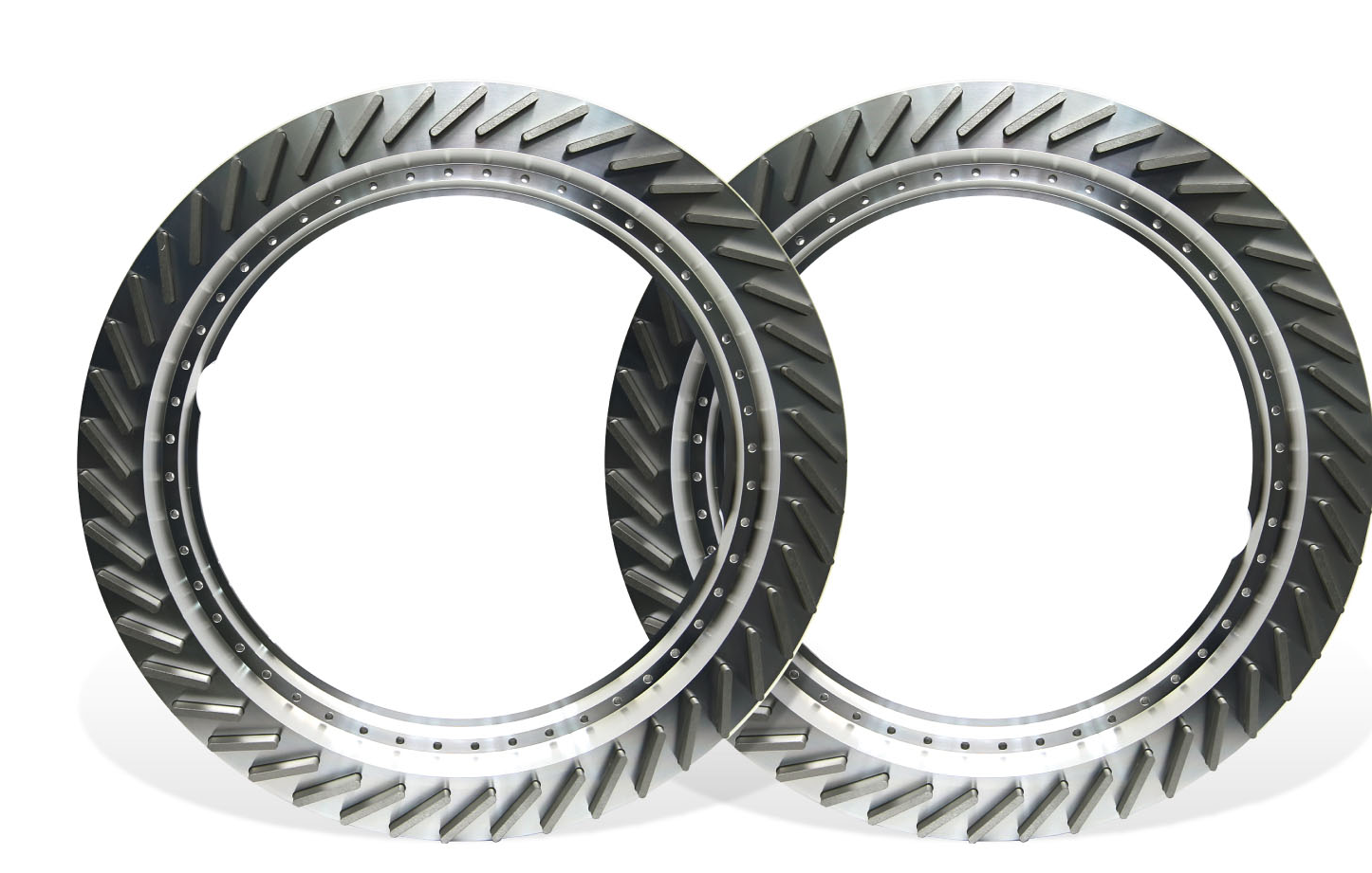
Q270 describes wheels for simultaneous grinding of multiple wafers, long life and high bulk removal. Suitable wheel designs and processing parameters are offered for different machines and grinding methods. Listed applications are silicon, sapphire, SiC, glass and hard materials such as zirconia. The diameter and segment ranges in this sheet are expressly kept separate from the earlier sapphire programme.
| Stage | Series | D [mm] | W [mm] | X [mm] | Grit |
|---|---|---|---|---|---|
| Rough | RS / MS Series | 200–380 | 2–5 | 3–10 | #170–#800 |
| Fine | SW Series | 200–380 | 2–5 | 3–10 | #1200–#4000 |

Microblades: bond, application and cutting surface
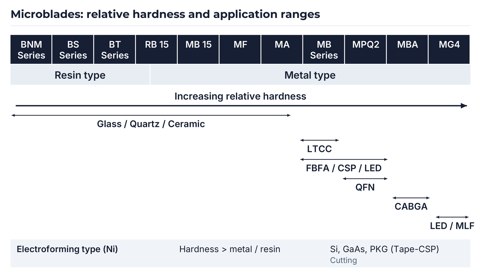
These thin precision blades target effective cutting at high rotational speeds and fast feed rates. Free-cutting versions support a stable cut and can reduce edge chipping. The selection matrix connects resin and metal versions with relative bond hardness and the application groups glass/quartz/ceramic, LTCC, FBFA/CSP/LED, QFN, CABGA and LED/MLF. All range arrows are retained; the Resin/Metal boundary lies within RB15.
The eleven designations are BNM Series, BS Series, BT Series, RB15, MB15, MF, MA, MB Series, MPQ2, MBA and MG4. The independent lower matrix row lists Electroforming Type, metal Ni, the hardness relation “Metal, Resin <”, and cutting of Si, GaAs and PKG (Tape-CSP). This row is not interpreted as an additional confirmed assignment to individual series.
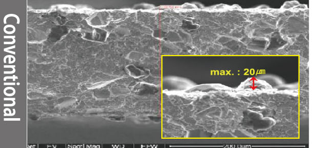
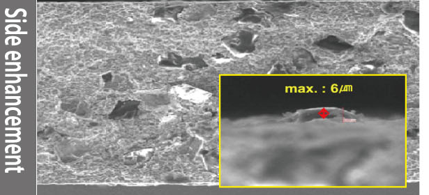
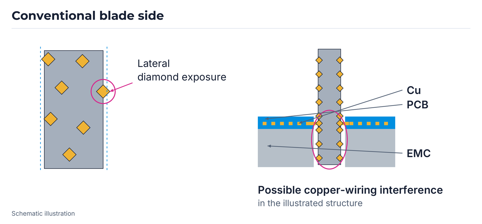
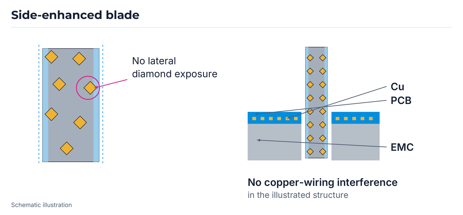
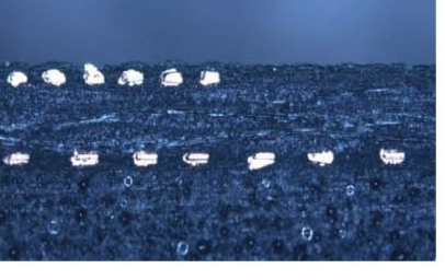
EHWA New Blade changes the side cutting surface. The comparison images specify a maximum of 20 µm for the conventional surface and 6 µm for side enhancement. These numbers describe the side feature marked in the detail image rather than the overall blade thickness. The conventional schematic shows exposed diamonds potentially interfering with copper wiring. The enhanced surface is shown without that interference. PCB, Cu and EMC regions and both actual cut images retain their individual assignments.

Dicing blades: cut geometry and chipping
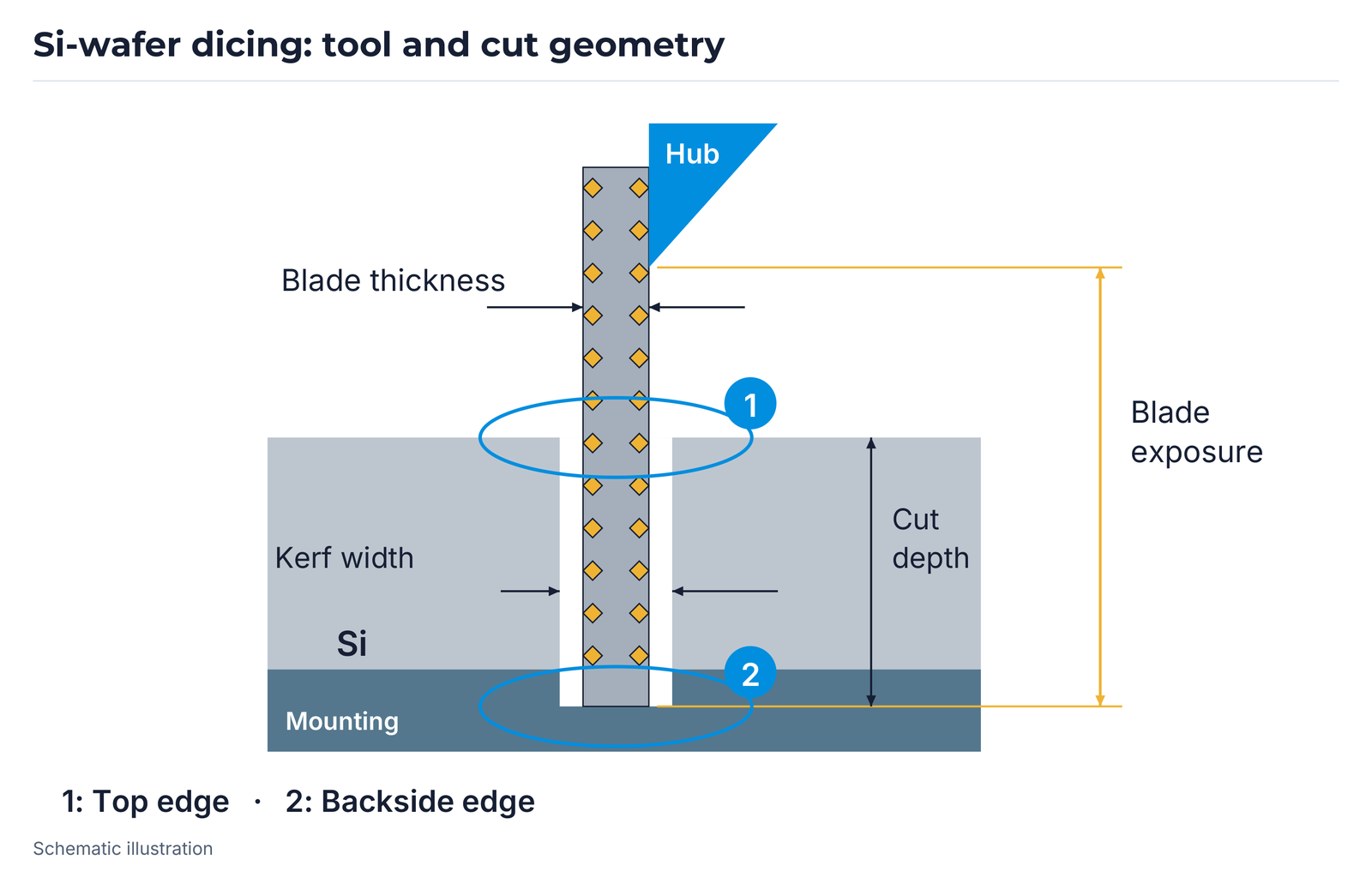
EHWA describes thin, precise blades with consistent quality supported by controlled grit-size distribution. Higher feed rates support productivity; tool and process are matched to the particular wafer and required cut appearance.
The silicon-wafer schematic distinguishes position 1 on the top side and position 2 on the back side. Blade thickness, kerf width, cut depth and free blade exposure remain separate quantities. The original associates finer grit with small top-side chipping, and coarser grit with effective cutting and lower load on individual grains at the back side. Cooling follows the machine and complete dicing process. The original sheet's blanket wet/dry assignment to the two wafer sides is not a general operating instruction.
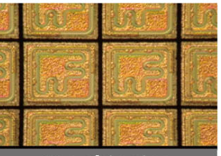
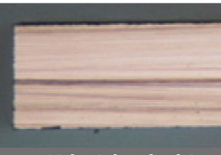
The new bond development is shown for silicon and compound semiconductors. Stated targets are small top, side and back chipping, and greater productivity through fast feeds. The two cut images show these separate assessment positions.
DP: wool felt, zirconia and process sequence
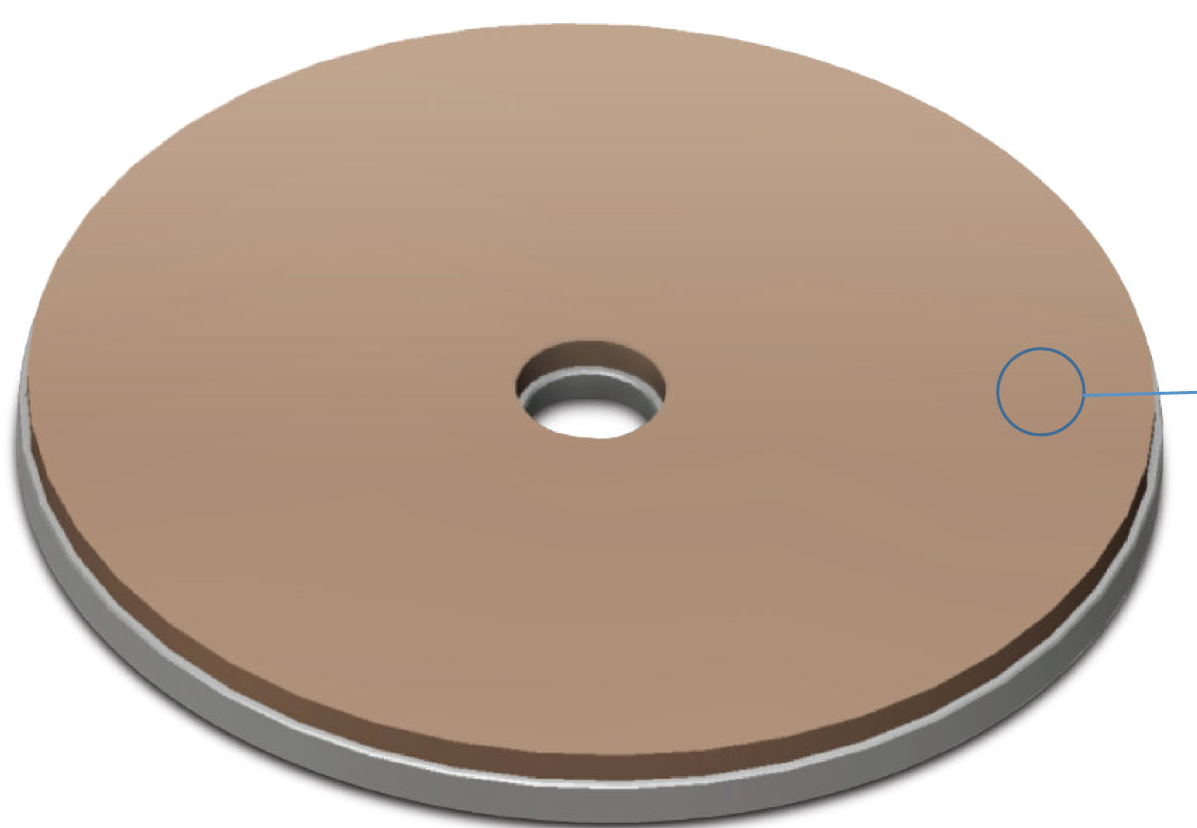
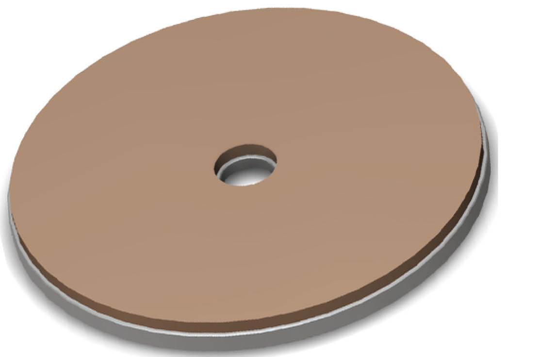
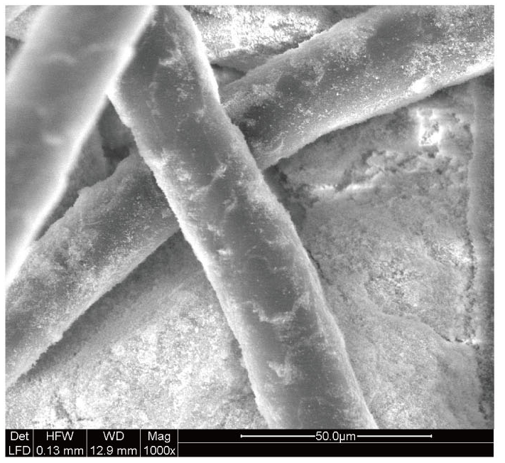
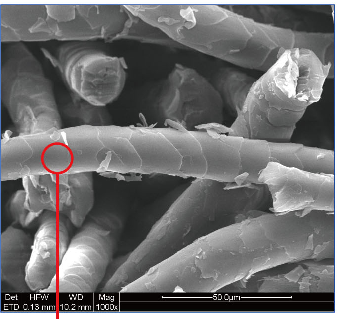
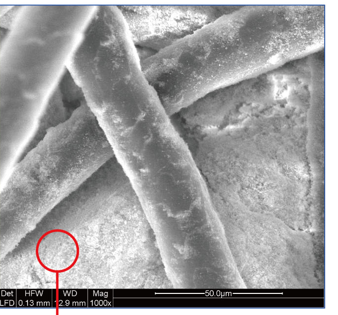
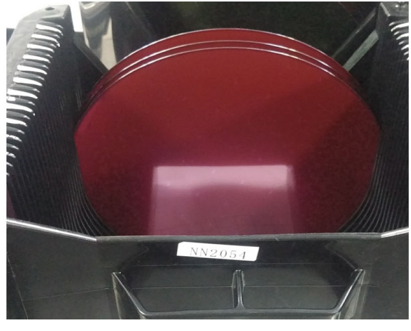
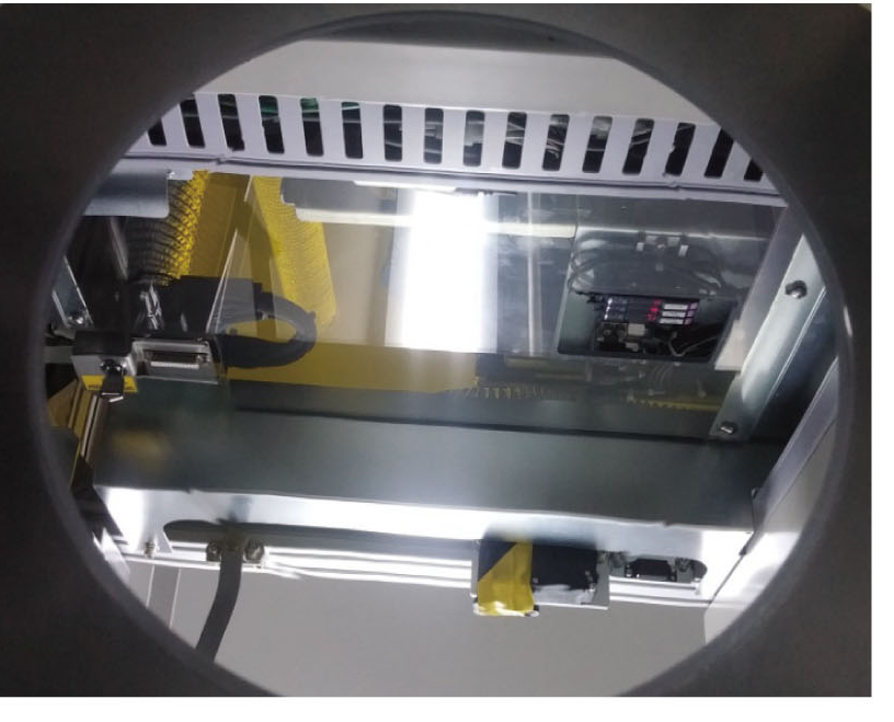
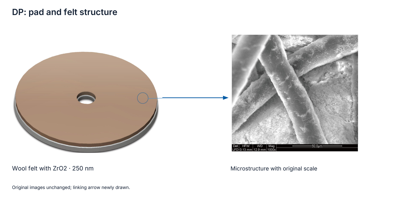
The DP dry-polishing pad combines wool felt with ZrO₂; the sheet specifies a size of 250 nm. The micrographs show felt before impregnation and the structure after impregnation with resin and ZrO₂. The workpiece images list 8- and 12-inch silicon wafers. The illustrated machine and two pad views supplement the particular application.
The three process stages retain their complete EHWA codes. DP provides surface finishing after grinding; polishing selection considers the incoming surface and the required strength and roughness levels.
| Stage | Q272 tool code |
|---|---|
| Z1 | EHWA BG01-D2-203D4.0W5X-325-RSL |
| Z2 | EHWA NP-D2-203D3.0W5X-5000J-VK8B |
| Z3 | EHWA DP-350D-LJC250 |
DP: two separate roughness measurements
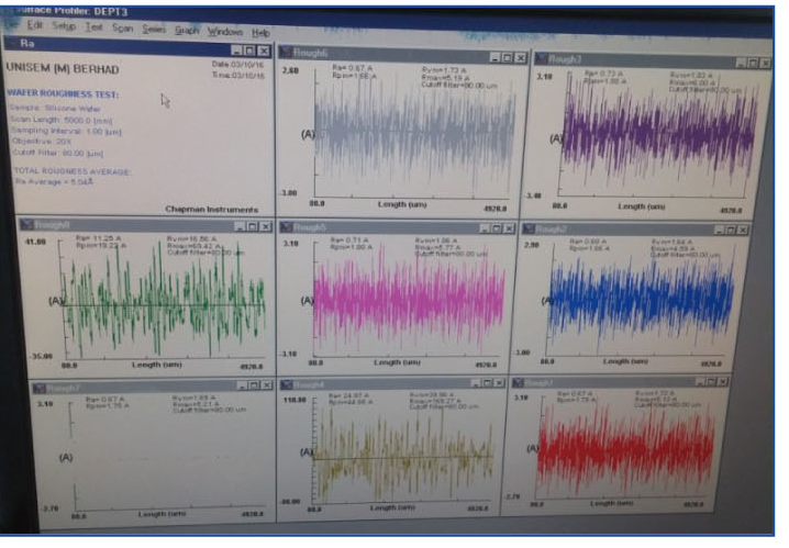
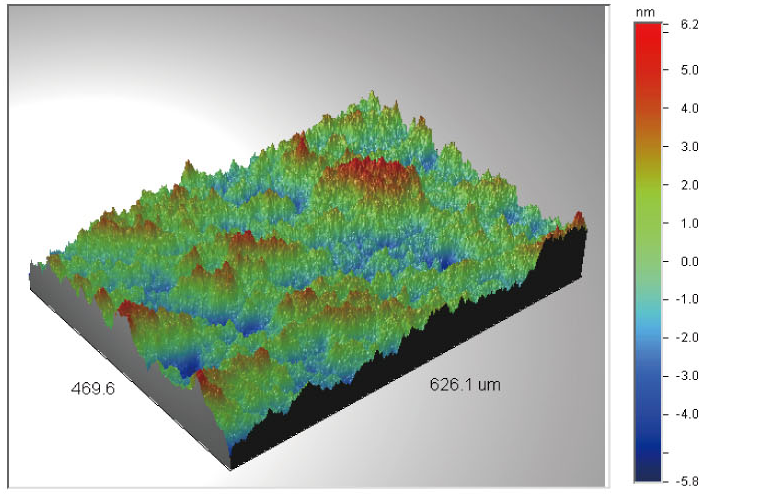
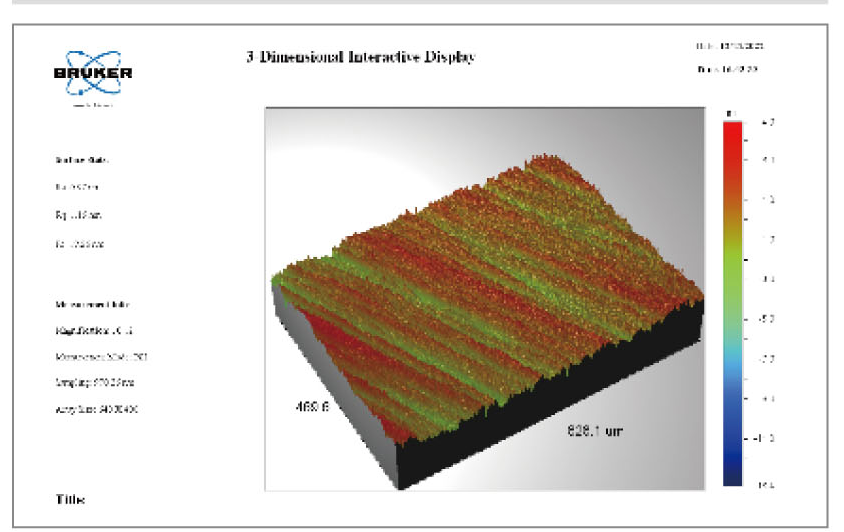
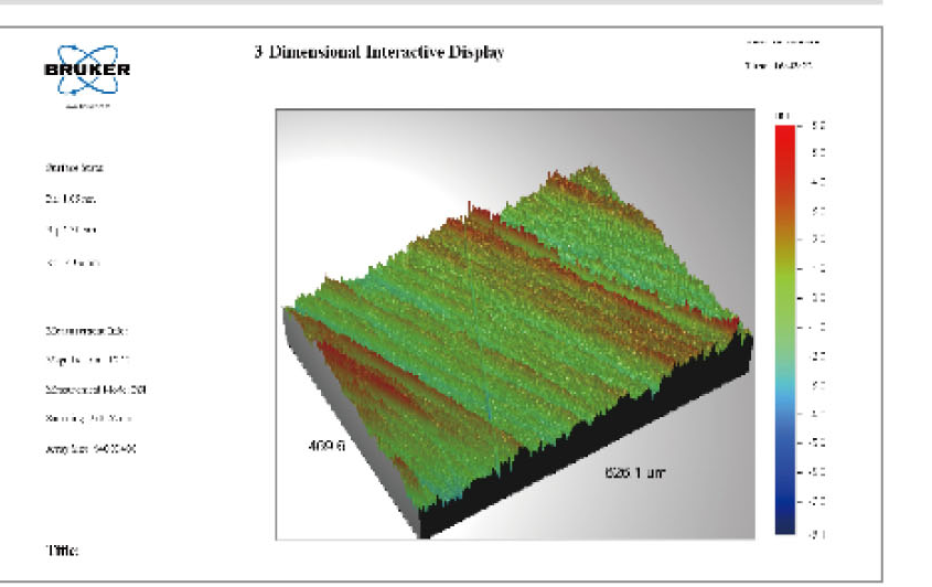
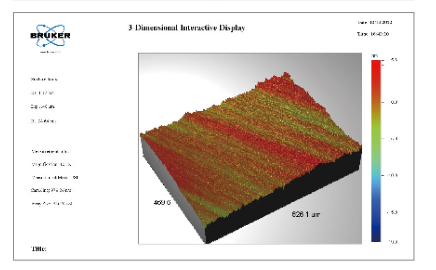
Q272 documents two measurement methods. The MP2000+ “Total Roughness Average” field gives Ra Average 5.04 Å. The typographic unit is confirmed by the corresponding original display in Q219/Q232. Optical 3D surface measurement using Wyko NT3300 instead gives Ra 1.17 nm, Rq 1.48 nm and Rt 11.97 nm. These results are kept separate because the measurement methods and evaluations differ. The original evaluations are retained as individual scientific images.
| Measurement method | Parameter | Value |
|---|---|---|
| MP2000+ | Sampling interval | 1.0 µm |
| MP2000+ | Objective | 20X |
| MP2000+ | Cutoff filter | 80.00 µm |
| MP2000+ | Ra Average | 5.04 Å |
| Wyko NT3300 / Optical 3D Surface | Ra | 1.17 nm |
| Wyko NT3300 / Optical 3D Surface | Rq | 1.48 nm |
| Wyko NT3300 / Optical 3D Surface | Rt | 11.97 nm |
Gettering dry-polishing pad: structure and trial
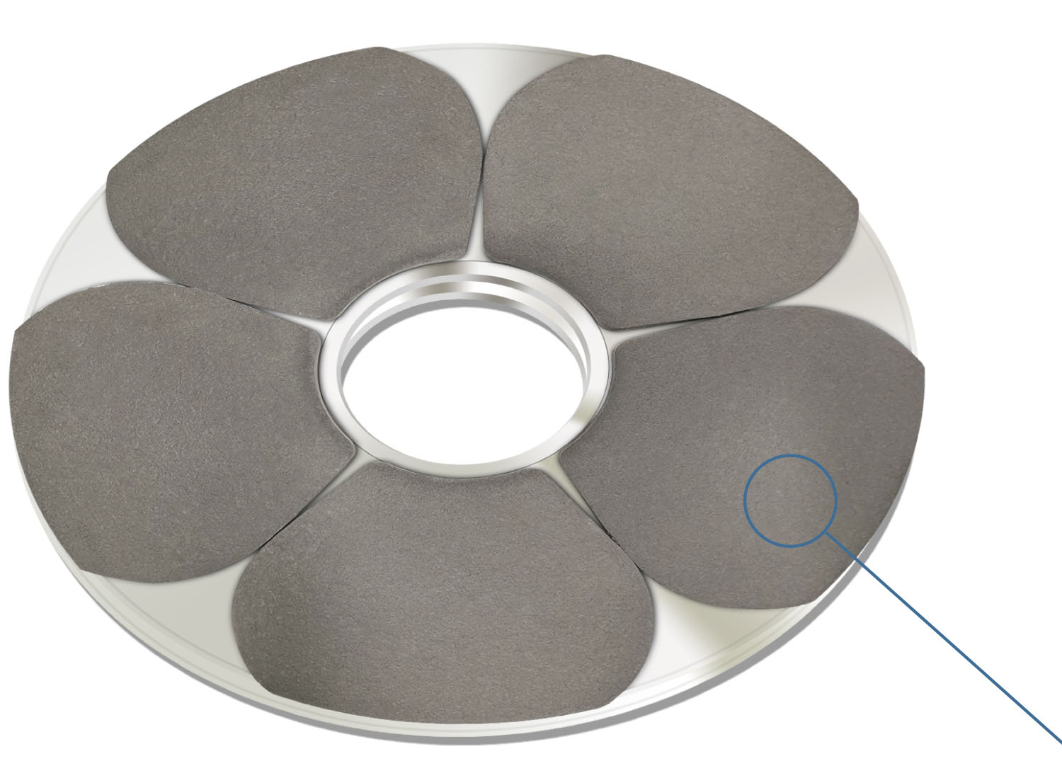
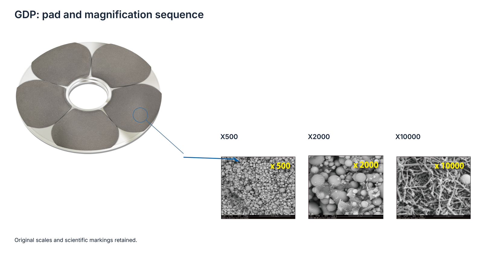
The combined sheet names the tool GDP – Gettering Dry Polishing Pad. Its bar chart additionally uses abbreviation GPP on the result axis. Both source designations remain identifiable; the trial is presented here under the expanded GDP product name. Gettering polishing combines surface processing with a gettering effect coordinated to the particular process. The general functional description comes from primary process documentation; it adds no unmeasured EHWA performance figures.
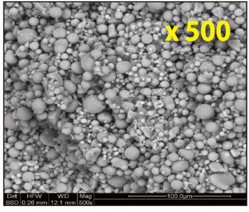
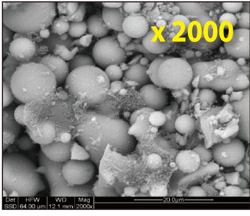
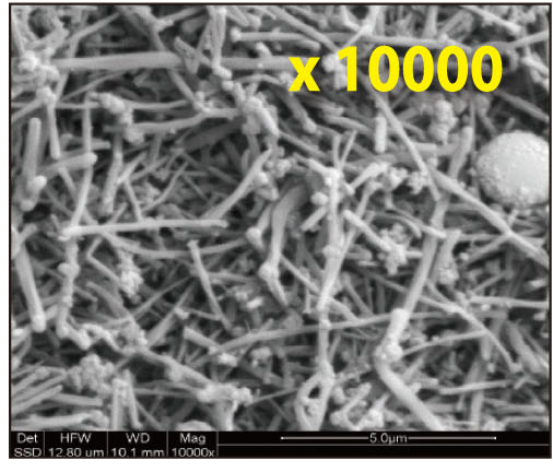
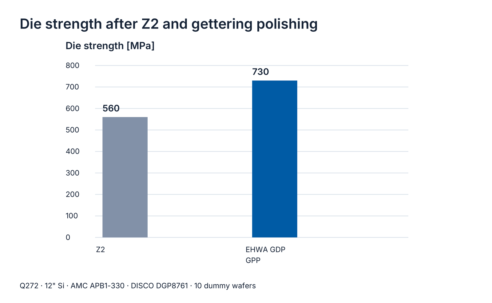
The trial processes 12-inch silicon with BG tape AMC APB1-330 on a DISCO DGP8761. The stated quantity is ten dummy wafers, not tool life. Z1 and Z2 are EHWA back-grinding tools; Z3 is the EHWA gettering polishing pad. The segmented pad geometry and micrographs at X500, X2000 and X10000 are retained.
Surface images are separated by position: centre Ra 0.92 nm, middle 1.05 nm and edge 1.17 nm. The die-strength comparison gives 560 MPa after Z2 and 730 MPa for EHWA GDP. These results belong to this process sequence.
Additional product views in the programme editions
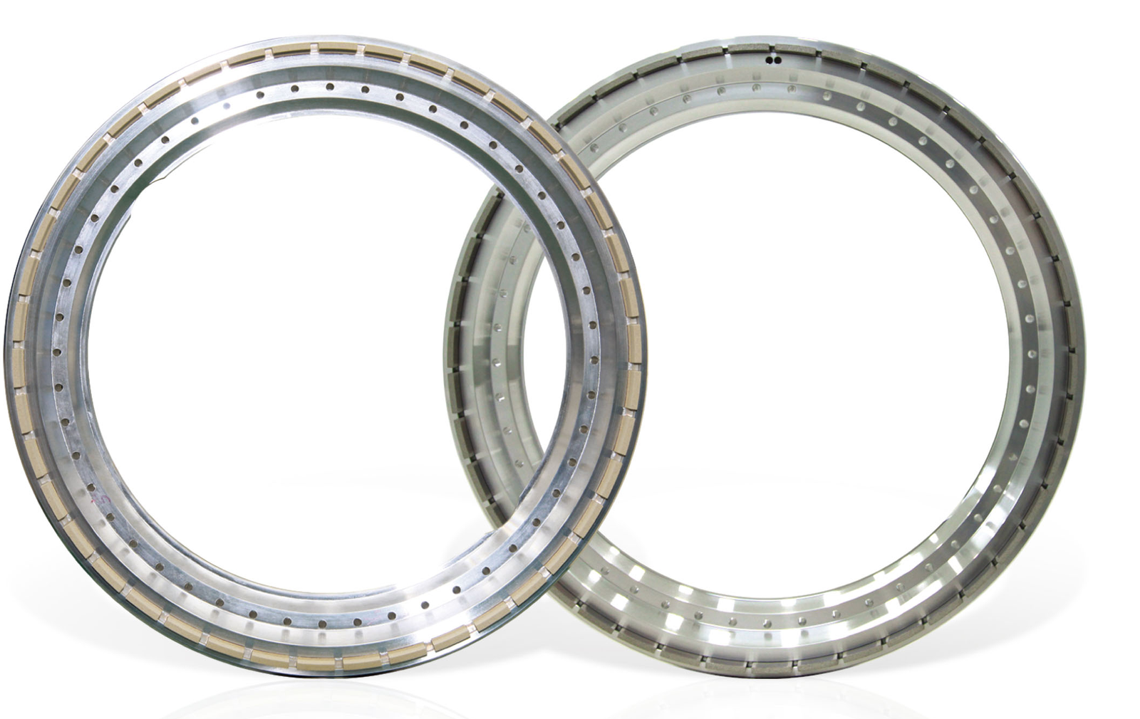
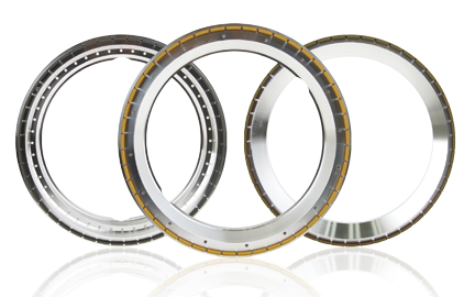
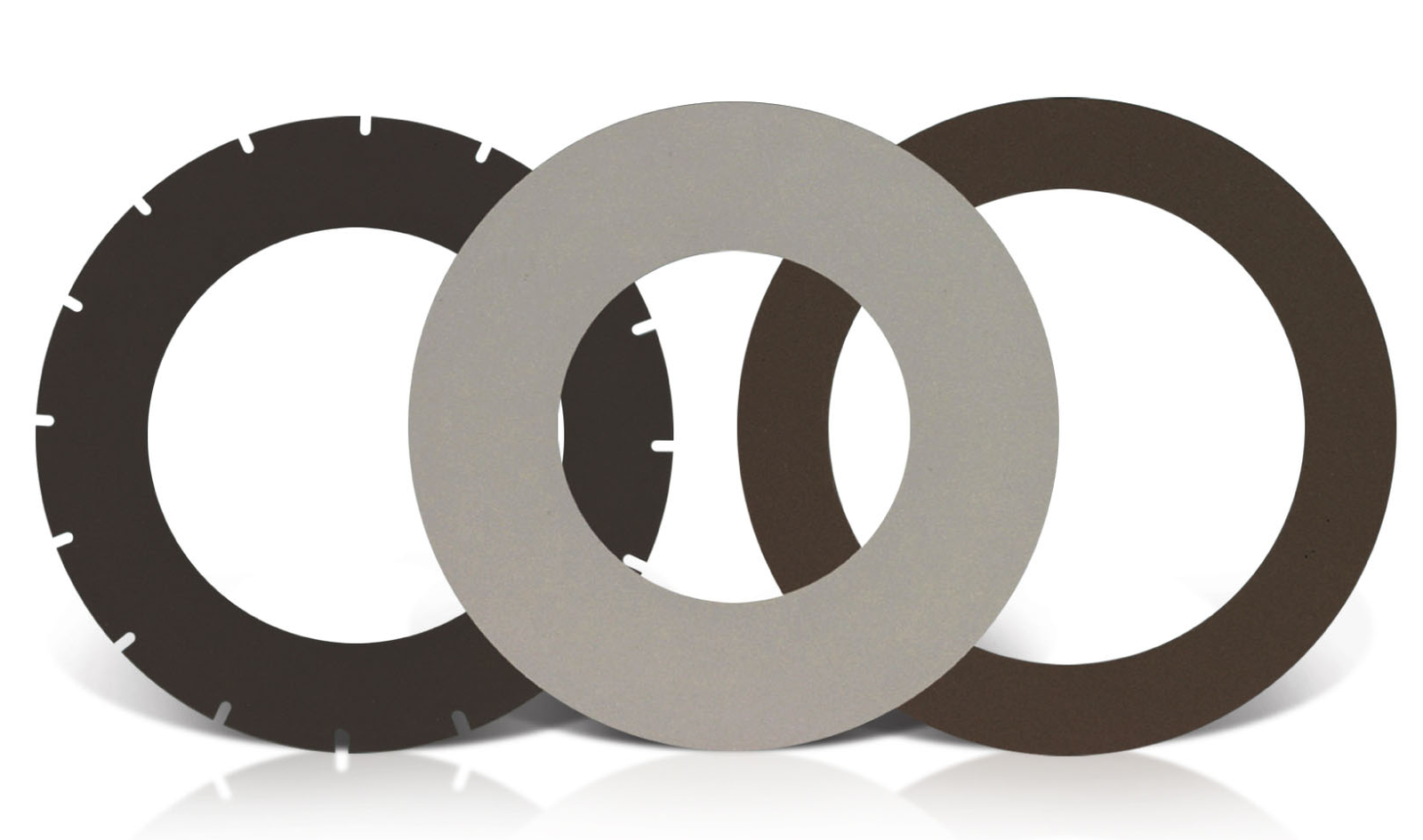
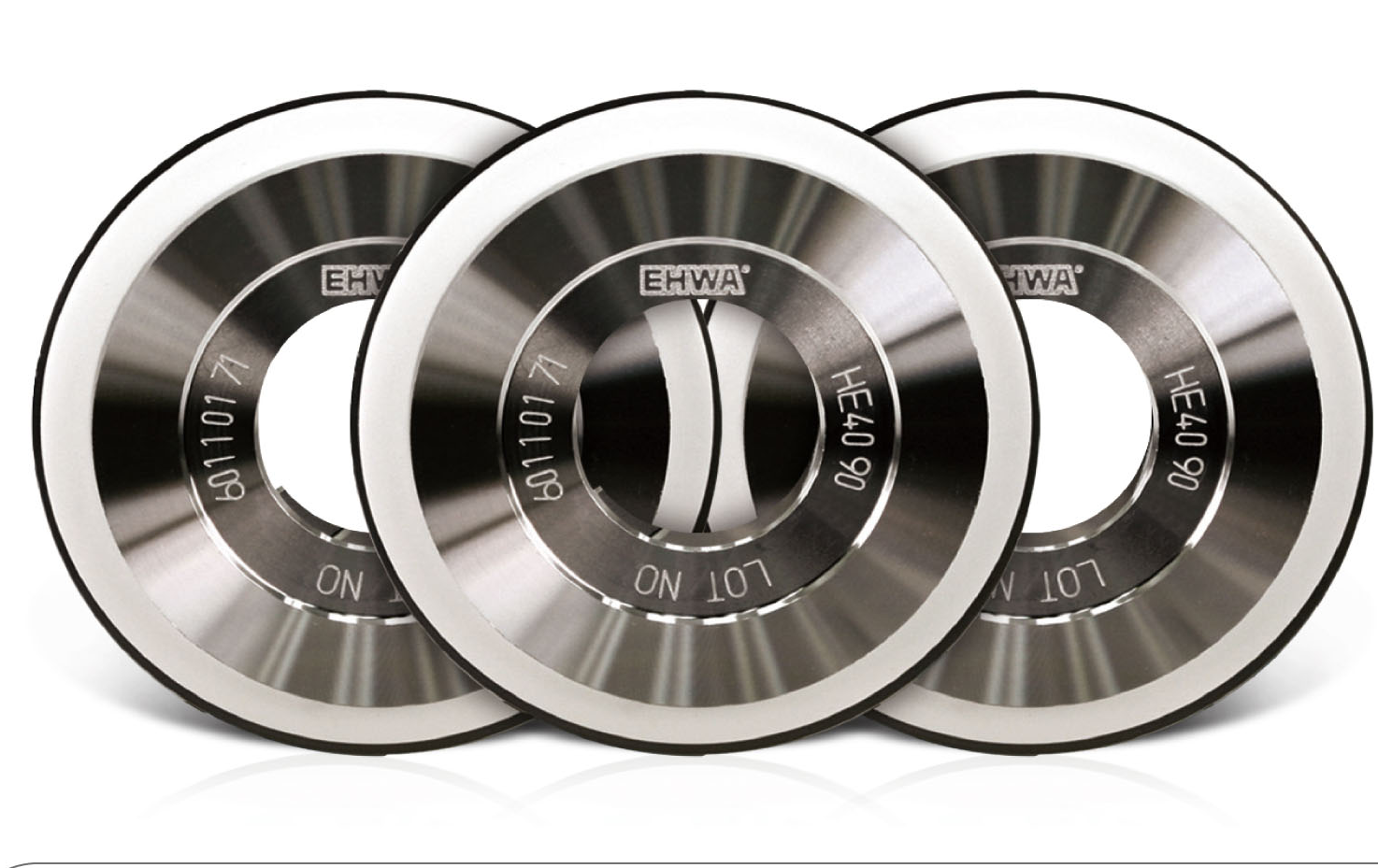
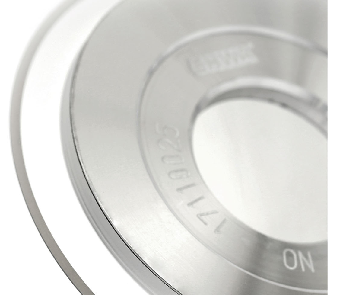
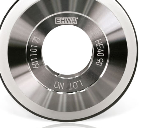
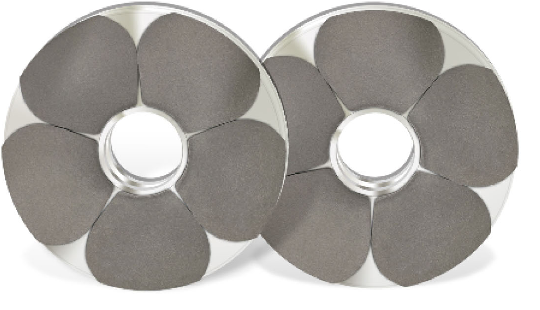
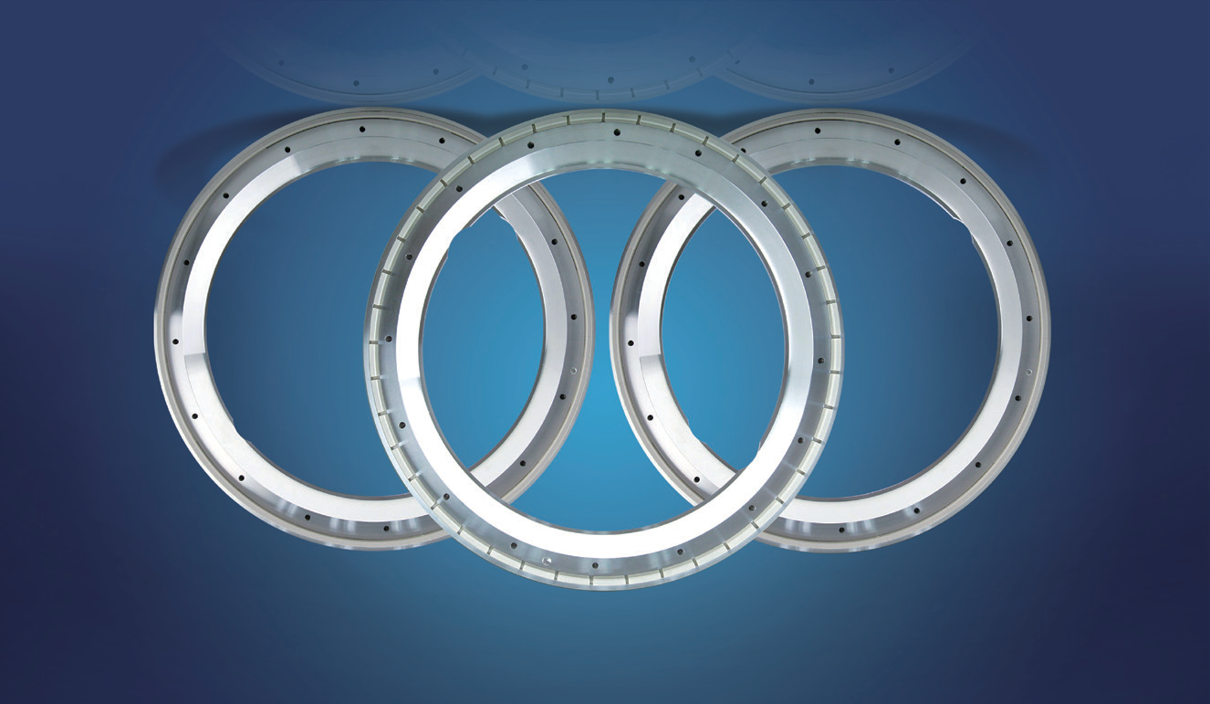
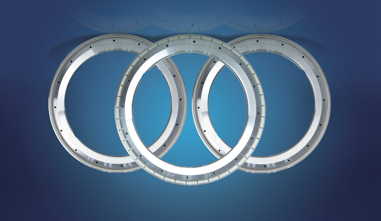
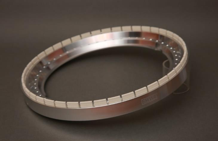
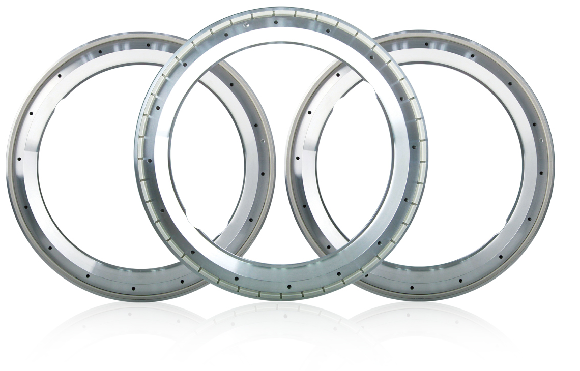
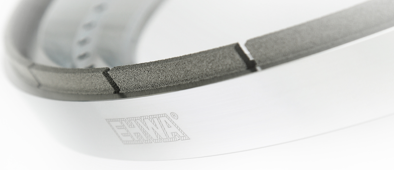
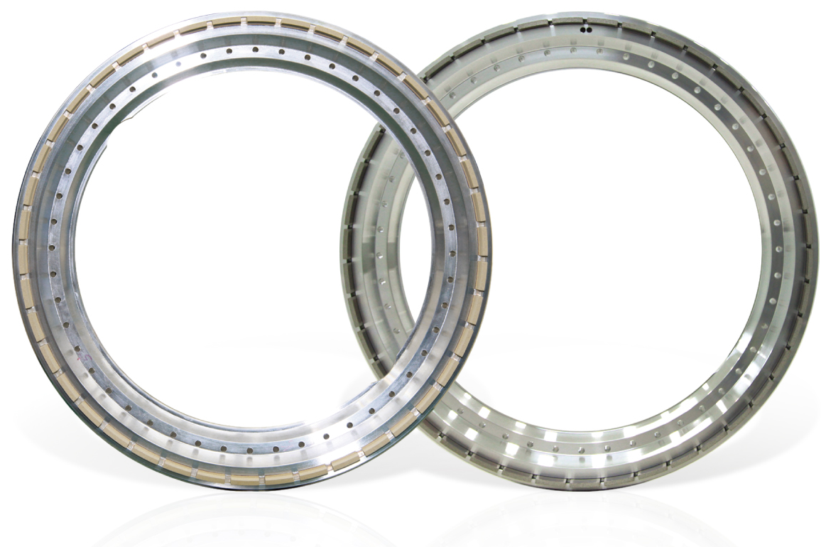
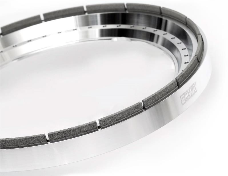
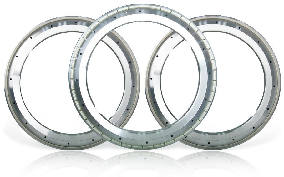
Programme sheets Q274 and Q275 use the same material-specific selection ranges as the complete main NANOPOL programme. Their independent tool views are retained. Q012 and Q026 show the earlier three-wheel group; Q221 adds a complete-wheel view and the recurring product group. Repeated decorative header images are presented once without removing technical product forms.


Development project named in the source
Q272 names “development of diamond tool technology and performance evaluation technology for manufacturing high-tech components”. It lists EHWA DIAMOND, PlanarSEMI, KITECH, Seoul National University and HANA Micron as participating organisations. The source note identifies Technology Innovation Program RS-2024-00455529, funded by Korea's Ministry of Trade, Industry and Energy (MOTIE). This is retained as project information from the sheet rather than a general certification or worldwide ranking claim.
Discuss your wafer-processing application
Provide the material structure, wafer diameter, initial and target thickness, machine and mounting. Existing Z1/Z2/Z3 codes, rotational speeds, feeds, grinding current, roughness measurement method and current wheel life help with selection. For compound wafers, add the simultaneously processed material constituents and observed loading or chipping. For cutting blades, kerf, free exposure and actual cooling arrangement are useful.
EHWA Europe: info@ehwadia.de · +49 6173 997780
Selection connects required removal, surface target and economical processing time. Start with the information already available; further details can be added during technical discussion.
Technical sources
The complete contents of the following twelve EHWA documents form the technical basis. Print dates are stated only where printed in the document. Trials retain their respective tools and conditions.
- EHWA: Sapphire Wafer Back Grinding Wheel 1 (printed 01/2017), pages 1–3.
- EHWA: NANO POL – Vitrified Back Grinding Wheel (printed 01/2017), pages 1–1.
- EHWA: NANO POL – Vitrified Back Grinding Wheel (second version, 01/2017), pages 1–1.
- EHWA: Sapphire Wafer Back Grinding Wheel (printed 01/2017), pages 1–3.
- EHWA: Back Grinding Wheel (printed 12/2018), pages 1–2.
- EHWA: NANOPOL – nine-page programme, pages 1–9.
- EHWA: NANOPOL – Semicon programme, pages 1–4.
- EHWA: Back Grinding Wheel, Micro Blade and Dicing Blade, pages 1–1.
- EHWA: DP, NANOPOL and GDP, pages 1–1.
- EHWA: NANOPOL – Compound Wafer Grinding Wheel, pages 1–1.
- EHWA: NANOPOL – Si Wafer Grinding Wheel, pages 1–1.
- EHWA: NANOPOL – complete ten-page programme, pages 1–10.