Dry polishing and gettering polishing after back grinding
Select the tool, surface and process together
EHWA offers polishing tools for finishing silicon wafers after back grinding. DP is used for dry polishing; GDP and GPP extend the range with configurations for gettering polishing. The examples show mirror surfaces, low roughness and increased die strength after the polishing step. Tool configuration, protective tape, machine and required backside structure are selected together.
| Range | Name | Illustrated application |
|---|---|---|
| DP | Dry Polishing Wheel | Dry polishing of silicon wafers; wool felt with ZrO₂, specified as 250 nm |
| GDP | Gettering Dry Polishing Wheel / Pad | Gettering dry polishing; different tool and machine examples |
| GPP | Gettering Polishing Pad | Gettering polishing; trial on 12-inch silicon wafers using DISCO DGP8761 |
In dry polishing, the polishing abrasive is contained in the tool; the polishing step does not require a separate polishing slurry. The process can reduce grinding damage on the wafer backside and support mechanical strength. Gettering also requires a suitable backside structure where impurities can be trapped. Low roughness alone does not demonstrate this function. The DP, GDP and GPP configurations are therefore described with their respective process examples.
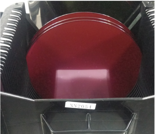
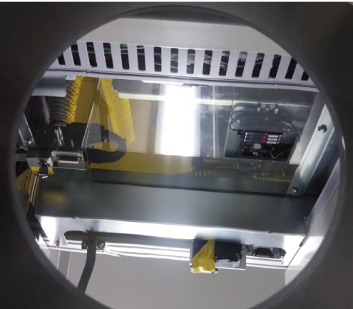
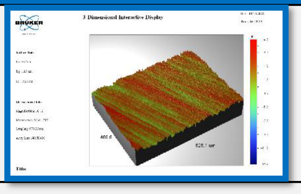
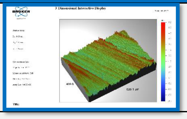
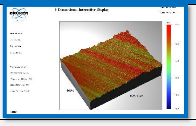
DP-350D: field trial and optical measurement
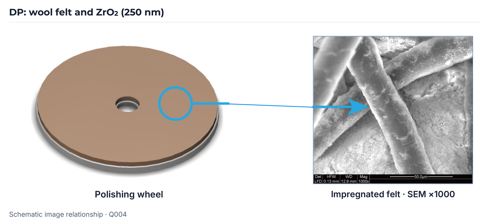
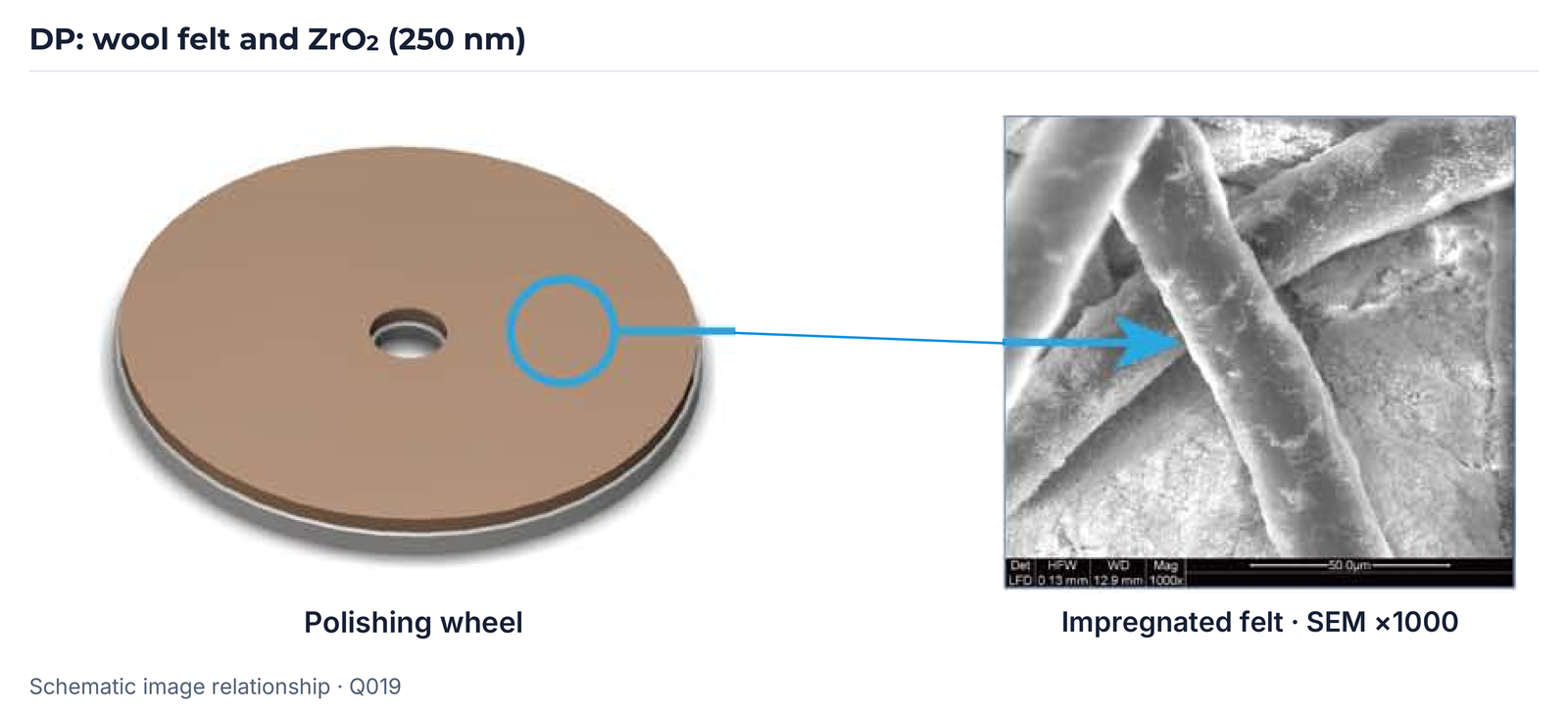
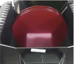
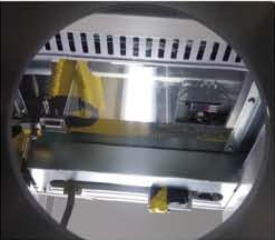
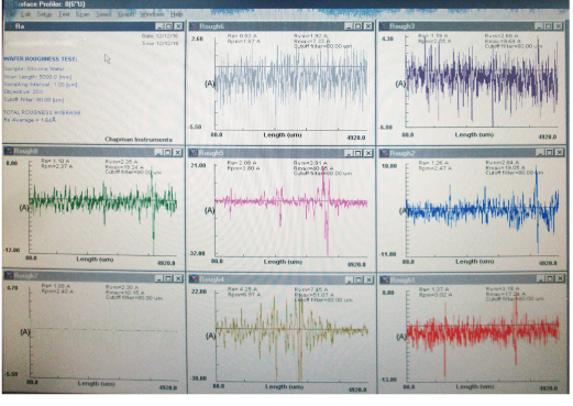
The DP configurations show wool felt with ZrO₂ (250 nm) for polishing silicon wafers. The process sequence uses EHWA back grinding wheels at Z1 and Z2, followed by EHWA DP-350D at Z3. Two DP documents contain this example at different image resolutions; the pictures from both versions are retained.
| Field trial | Q004 | Q019 |
|---|---|---|
| Sampling interval | 1.0 µm | 1.0 µm |
| Objective | 20× | 20× |
| Cutoff filter | 80.00 µm | 80.00 µm |
| Measuring instrument | MP2000+ | MP2000+ |
| Average roughness, Ra Average | 1.64 Å | 1.64 Å |
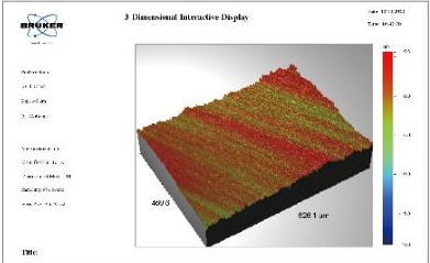
| Separate optical measurement | Q004 / Q019 |
|---|---|
| Ra | 1.17 nm |
| Rq | 1.48 nm |
| Rt | 11.97 nm |
| Measuring instrument | Wyko NT3300 |
| Method | Optical 3D surface measurement |

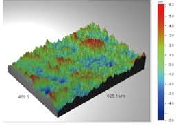
The results come from different measurement setups. The field trial value in Å and the optical measurement values in nm are presented separately.
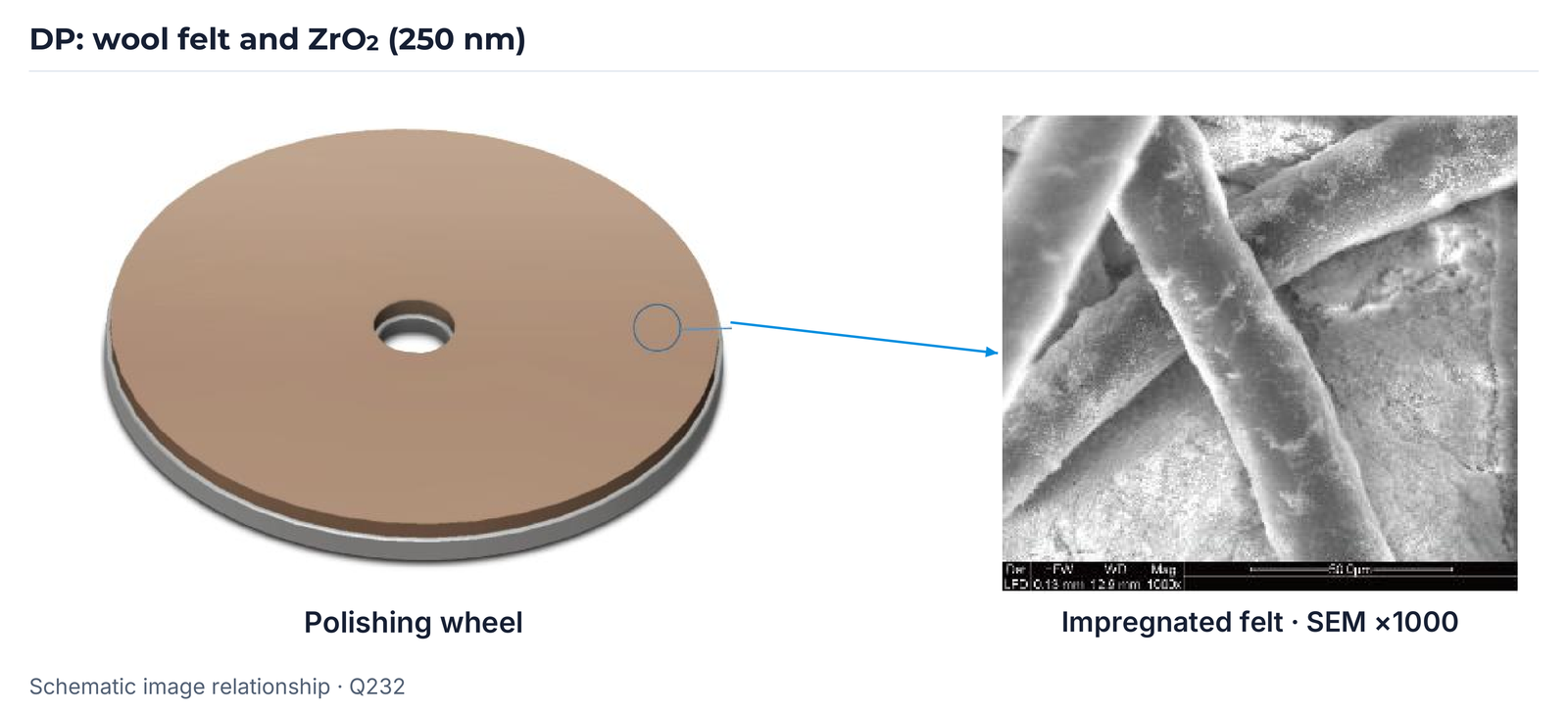
DP: wool felt and impregnation
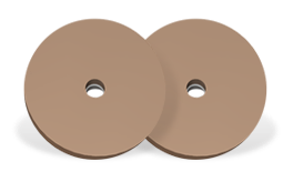
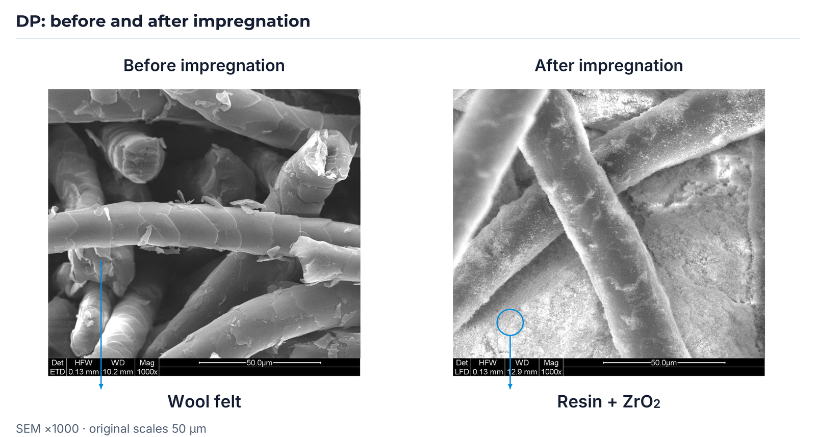
The detailed DP presentation describes wool felt and ZrO₂ (250 nm). Before impregnation, the SEM photograph shows the felt fibres; after impregnation, the surface is labelled as resin with ZrO₂. The embedded original scales are 50 µm in both photographs at ×1000 magnification.

DP-350D-LJC250: process for 8- and 12-inch wafers
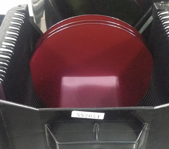
The application example specifies 8- and 12-inch silicon wafers. The tool sequence includes the complete specifications for back grinding and the final DP step:
| Station | EHWA tool |
|---|---|
| Z1 | BG01-D2-203D4.0W5X-325-RSL |
| Z2 | NP-D2-203D3.0W5X-5000J-VK8B |
| Z3 | DP-350D-LJC250 |

DP: roughness in the detailed process example
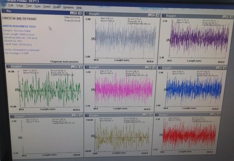
| Field measurement from Q219, page 4 | Specification |
|---|---|
| Sampling interval | 1.0 µm |
| Objective | 20× |
| Cutoff filter | 80.00 µm |
| Measuring instrument | MP2000+ |
| Average roughness, Ra Average | 5.04 Å |
| Separate optical measurement from Q219 | Specification |
|---|---|
| Ra | 1.17 nm |
| Rq | 1.48 nm |
| Rt | 11.97 nm |
| Measuring instrument | Wyko NT3300 |
| Method | Optical 3D surface measurement |
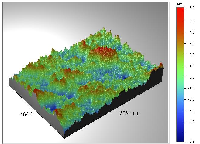
The 5.04 Å field value belongs to this example; the shorter DP-350D documents specify 1.64 Å. The differences are retained as variants of the respective trial documents. They do not establish a common performance limit.
DP: additional presentation of the tool sequence and measurements
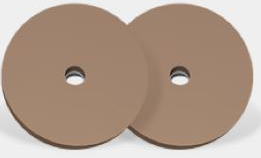
The DP section of the GPP / DP document also shows wool felt and ZrO₂ (250 nm), the before-and-after impregnation comparison, and 8- and 12-inch silicon wafers. The illustrations and tool codes of this version are included in full.

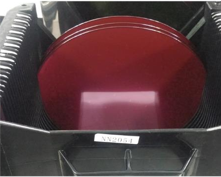
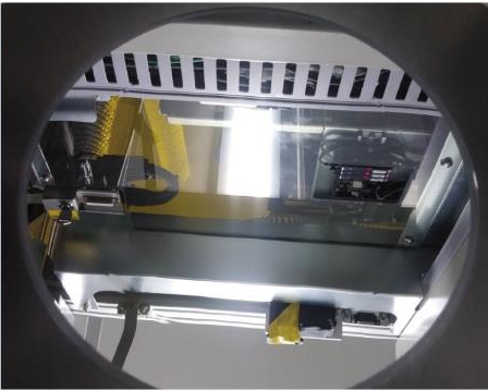
| Station | Tool from Q232, page 3 |
|---|---|
| Z1 | BG01-D2-203D4.0W5X-325-RSL |
| Z2 | NP-D2-203D3.0W5X-5000J-VK8B |
| Z3 | DP-350D-LJC250 |
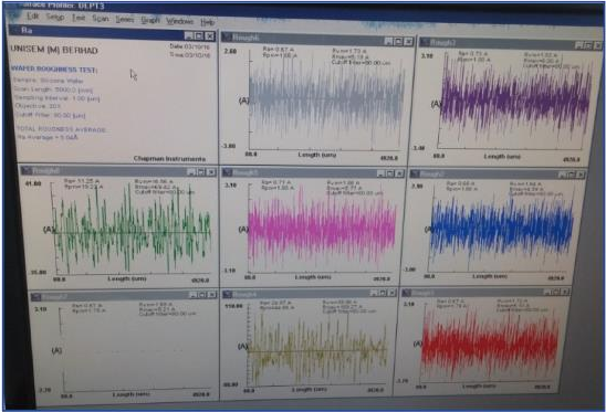
| Field measurement from Q232, page 4 | Specification |
|---|---|
| Sampling interval | 1.0 µm |
| Objective | 20× |
| Cutoff filter | 80.00 µm |
| Measuring instrument | MP2000+ |
| Average roughness, Ra Average | 5.04 Å |
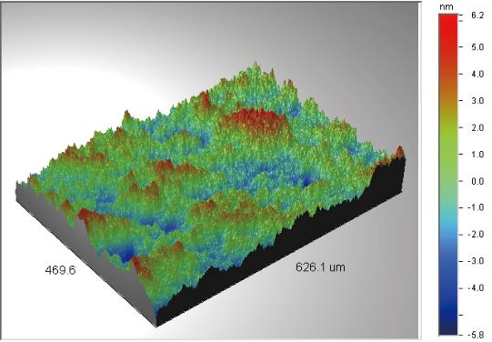
| Separate optical measurement from Q232 | Specification |
|---|---|
| Ra | 1.17 nm |
| Rq | 1.48 nm |
| Rt | 11.97 nm |
| Measuring instrument | Wyko NT3300 |
| Method | Optical 3D surface measurement |
GDP 450D-26T-130H: process and microstructure
The GDP “Sample 1” example describes 12-inch silicon wafers, a Lintec protective tape and the machines listed below. The microstructure is illustrated at ×500, ×2000 and ×10000 magnification; the original scales are 100, 20 and 5 µm. Q005 and Q022 contain the same confirmed identical page, presented together here.
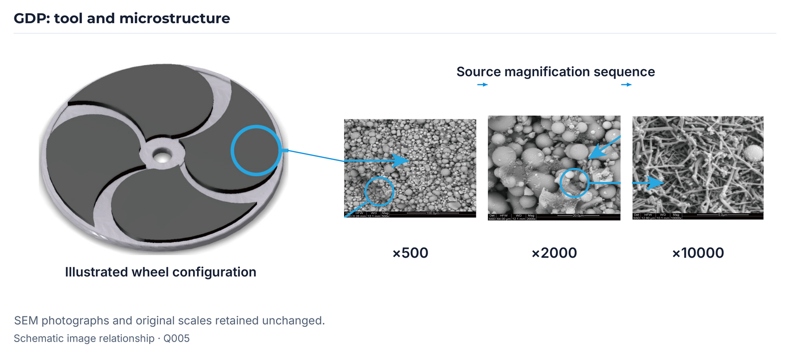
| Trial condition | GDP “Sample 1” |
|---|---|
| Workpiece | Silicon wafer, 12 inches |
| Back grinding tape | Lintec P-7180 (180 µm) |
| Machine specification | DGP 8761 (NN2412) & DFM2800 |
| Quantity | 10 dummy wafers |
| Z1 | EHWA Back Grinding Wheel |
| Z2 | EHWA Back Grinding Wheel |
| Z3 | EHWA-GDP 450D-26T-130H |
GDP: TEM preparation and damage depth
A specimen is removed from the wafer for examination. The preparation diagram identifies a depth of 6 µm and another specimen dimension of 6 µm. The subsequent TEM image is specified at ×12000 magnification. It distinguishes carbon tape for TEM, Pt coating for TEM, the etched surface and the width of the recess.


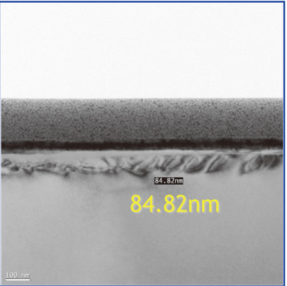
The reported damage depth is 84.82 nm. It describes the illustrated TEM finding in this GDP trial; it is not a general limit for other GDP configurations.
GDP 300D-26T: another machine trial
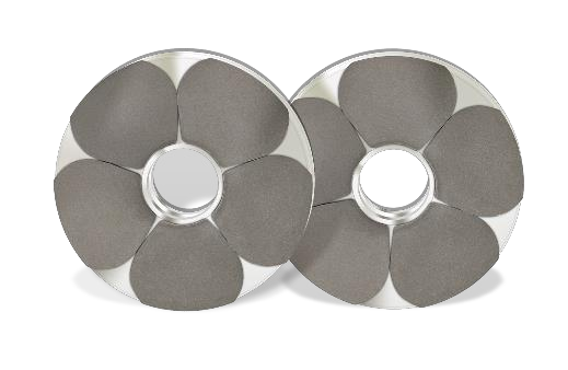
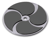
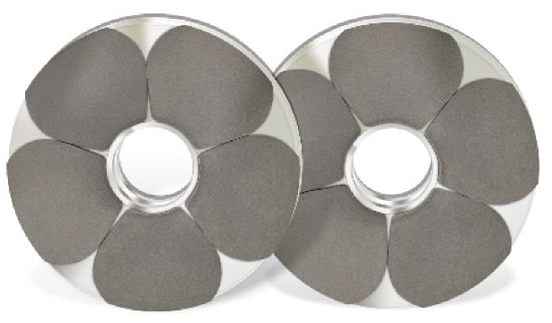
Another GDP configuration shows a wheel with five polishing areas and a wheel pair. The three SEM structures are labelled ×500, ×2000 and ×10000; their sequence is additionally identified by 1, 2 and 3.
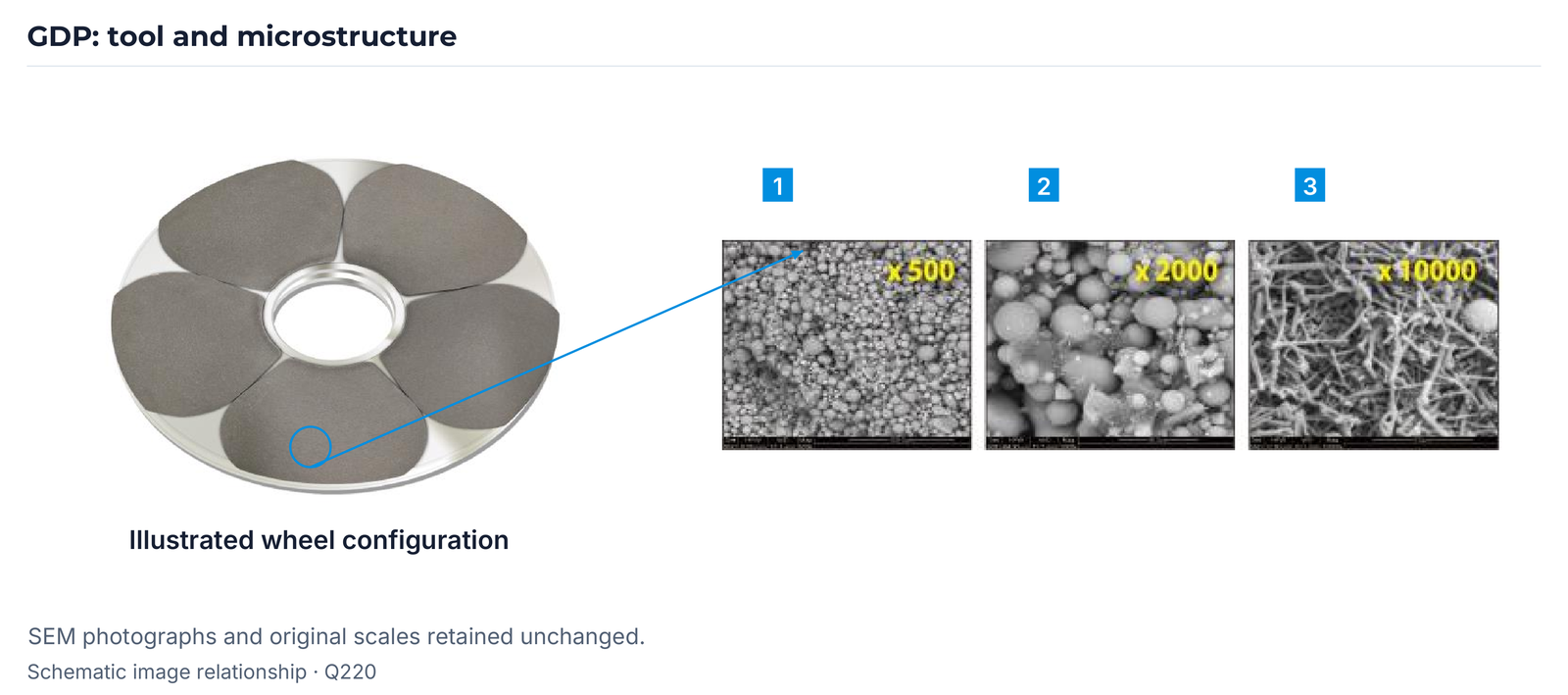
| Trial condition | GDP from Q220 |
|---|---|
| Workpiece | Silicon wafer, 12 inches |
| Back grinding tape | AMC APB1-330 |
| Machine | INSEMITEC IVG 3030 |
| Quantity | 10 dummy wafers |
| Z1 | EHWA Back Grinding Wheel |
| Z2 | EHWA Back Grinding Wheel |
| Z3 | EHWA-GDP 300D-26T |
GDP: surface roughness and die strength
| Measurement position | Ra in the GDP trial from Q220 |
|---|---|
| Center | 0.92 nm |
| Middle | 1.05 nm |
| Edge | 1.17 nm |
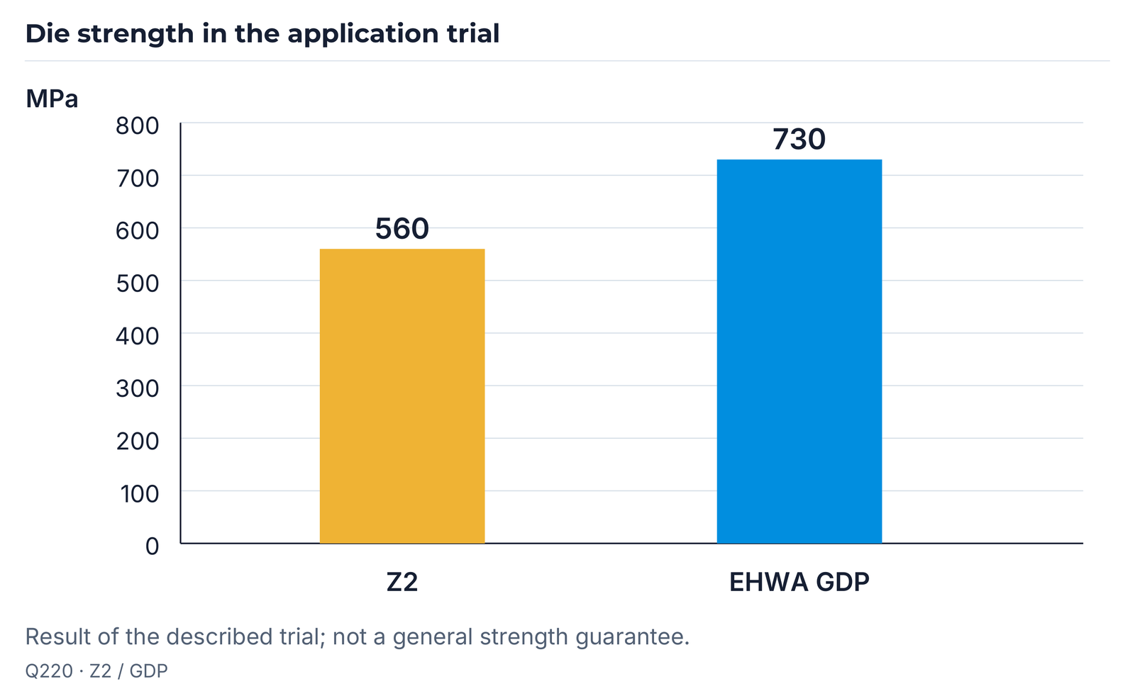
The strength comparison specifies 560 MPa after Z2 and 730 MPa for EHWA GDP. It shows higher die strength after the GDP step in the described trial. The test is labelled “Die Strength”; the test method and final thickness are not detailed here.
| Comparison | Die strength |
|---|---|
| Z2 | 560 MPa |
| EHWA GDP | 730 MPa |
GPP: Gettering Polishing Pad
The GPP example shows a configuration with five polishing areas, a wheel pair and three SEM structures at ×500, ×2000 and ×10000. The corresponding original scales are 100, 20 and 5 µm. A DISCO DGP8761 process is specified for this example.

| Trial condition | GPP from Q232 |
|---|---|
| Workpiece | Silicon wafer, 12 inches |
| Back grinding tape | AMC APB1-330 |
| Machine | DISCO DGP8761 |
| Quantity | 10 dummy wafers |
| Z1 | EHWA Back Grinding Wheel |
| Z2 | EHWA Back Grinding Wheel |
| Z3 | EHWA-Gettering Polishing Pad |
GPP: surface measurement and strength comparison
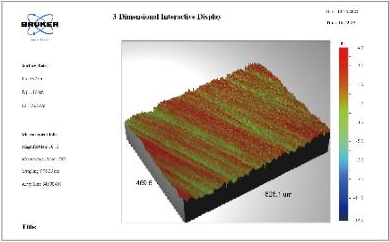
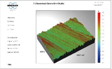
| Measurement position | Ra in the GPP trial from Q232 |
|---|---|
| Center | 0.92 nm |
| Middle | 1.05 nm |
| Edge | 1.17 nm |
| Comparison | Die strength |
|---|---|
| Z2 | 560 MPa |
| EHWA GPP | 730 MPa |
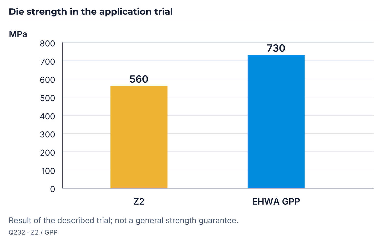
The comparison shows higher die strength after the GPP step under the described trial conditions. The figures belong to the GPP example; matching results in the separate GDP example do not establish that the tools are generally equivalent. The test method and final thickness are not specified in this presentation.
GDP pad: additional tool presentation
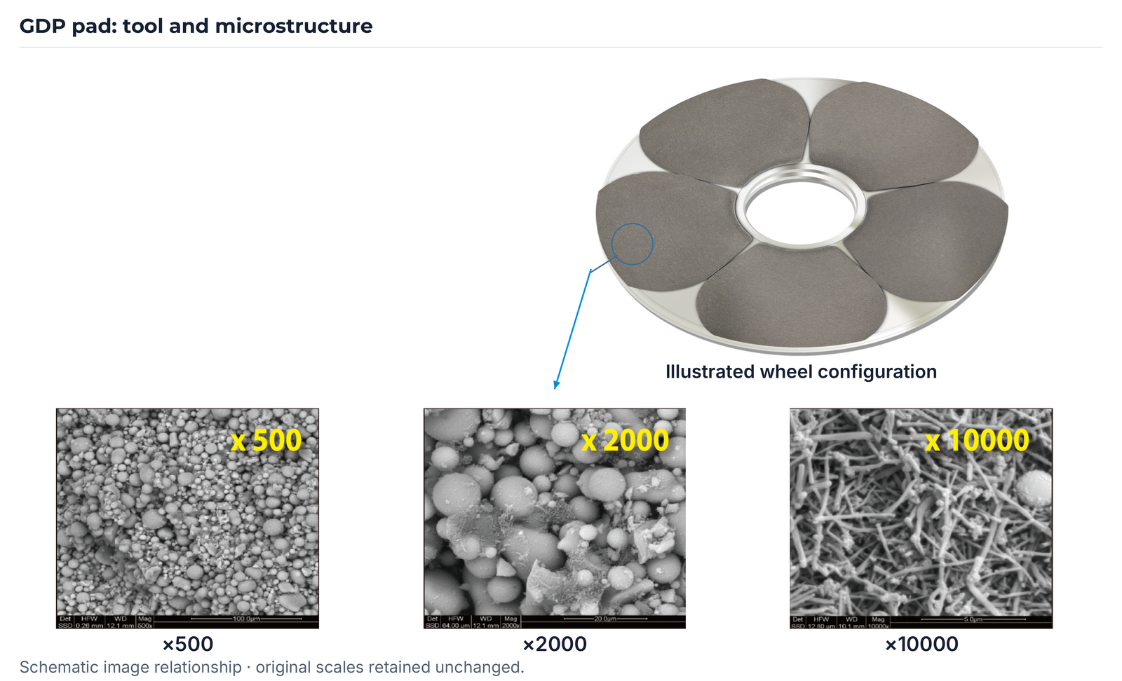
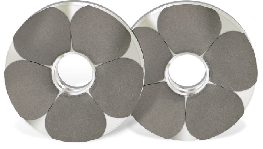
The additional GDP pad document specifies the same “EHWA-Gettering Polishing Pad” name for Z3 and shows a wheel with five polishing areas, a wheel pair and SEM structures at ×500, ×2000 and ×10000. It contains the following process conditions without adding separate roughness or strength values:
| Trial condition | GDP pad from Q273 |
|---|---|
| Workpiece | Silicon wafer, 12 inches |
| Back grinding tape | AMC APB1-330 |
| Machine | DISCO DGP8761 |
| Quantity | 10 dummy wafers |
| Z1 | EHWA Back Grinding Wheel |
| Z2 | EHWA Back Grinding Wheel |
| Z3 | EHWA-Gettering Polishing Pad |
Adapt the polishing process to your wafers
To select the tool, provide wafer material and diameter, initial and final thickness, frontside structure, protective tape, machine and Z1 / Z2 tools. Add the required roughness with measurement method and positions, together with requirements for die strength, gettering, stock removal and cycle time. EHWA Europe can help match the tool and process to this information.
Technical enquiry to EHWA Europe · Telephone +49 6173 99778-0
Technical basis
EHWA documents: Dry Polishing Wheel DP (Q004 and Q019, 1 page each); GDP Wheel (Q005 and Q022, 1 identical page each); DP Wheel (Q219, pages 1–4); GDP Wheel (Q220, pages 1–2); GPP / DP (Q232, pages 1–4); GDP Gettering Dry Polishing Pad (Q273, 1 page). All reported trial values apply to the respective investigation described.
The additional process explanation is supported by DISCO: dry polishing and DISCO: Gettering DP. These sources explain the process; their separate product and trial values are not transferred into the EHWA tables.