Dicing and microblades for electronic components
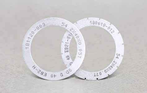
EHWA develops thin diamond blades for silicon wafers, compound semiconductors, electronic packages and hard, brittle materials. Hub blades, free-standing metal- or resin-bonded microblades and electroformed nickel blades offer different ways to match kerf width, cut quality and productivity to the component.
Development targets precise cuts, reduced chipping and consistent machining quality. Controlled abrasive particle-size distribution supports these goals; high feed speeds can improve productivity. EHWA tailors the blade configuration to the customer application.
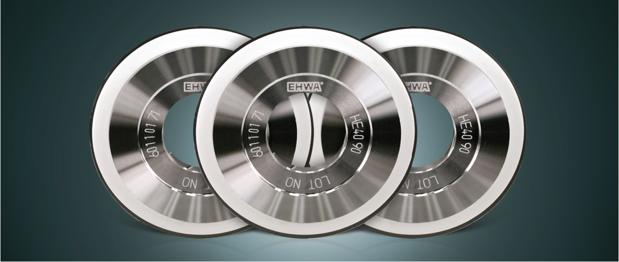
Hub dicing blades
The dicing blades combine high manufacturing accuracy with a very thin cutting section. New bond development addresses silicon and compound semiconductors. Reduced top- and backside chipping and high feed speeds are central development goals.
Cut geometry and edge chipping
Blade thickness describes the cutting body. Kerf width refers to the resulting slot in the workpiece and is shown as a separate dimension. Blade exposure extends from the hub to the cutting end; cut depth is measured from the wafer top surface to the cutting end. The mounting lies beneath the silicon wafer. The top and backside edges may exhibit different chipping mechanisms.
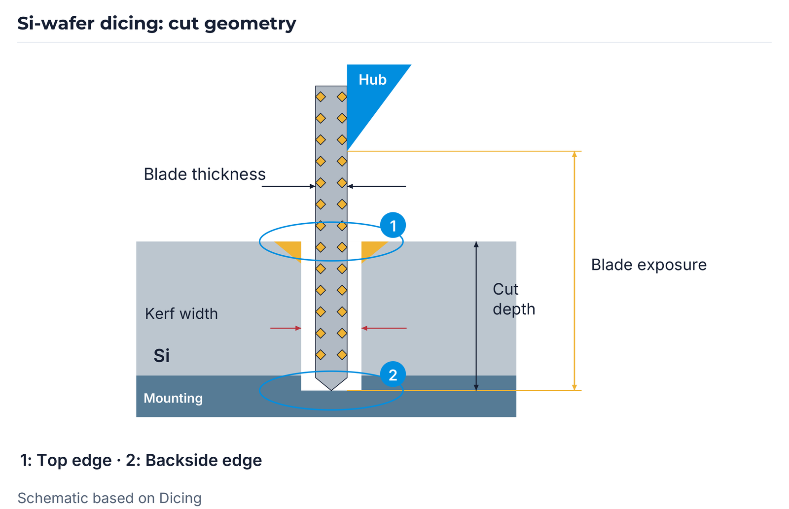
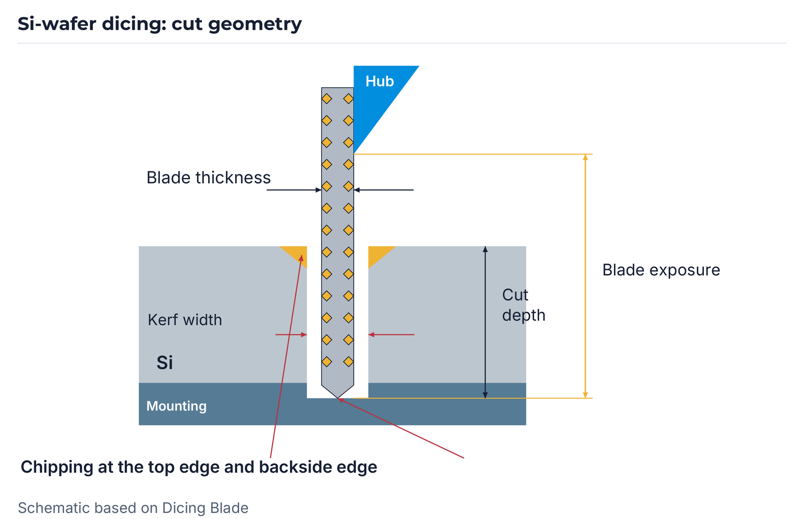
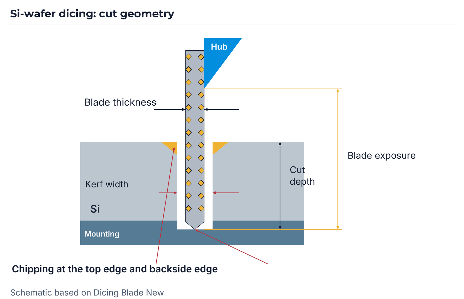
| Area | Comparison in the dicing product sheets |
|---|---|
| Wafer top side | Wet cutting with coolant; fine diamond grit is associated with small top-side chips. |
| Wafer backside | The illustrated model contrasts dry cutting without coolant and coarser diamond grit, with high cutting ability and reduced load on each grit. |
This comparison describes the model in the dicing product sheets. For thin wafers, finer grit can also reduce backside chipping. Grit size, feed speed, spindle speed, workpiece thickness, coolant and mounting must therefore be matched together to the specific cut. Coolant conditions follow the approved machine and application process.
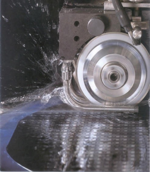
New bonds for silicon and compound semiconductors
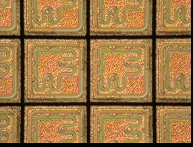
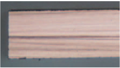
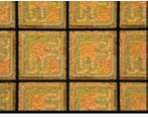
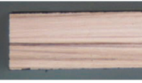
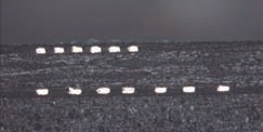
The illustrated bond development combines reduced top- and backside chipping with the ability to operate at high feed speeds. The application images below show the top side and the side/backside cut zone. The images do not specify a numeric chipping limit.
Microblades: applications and benefits
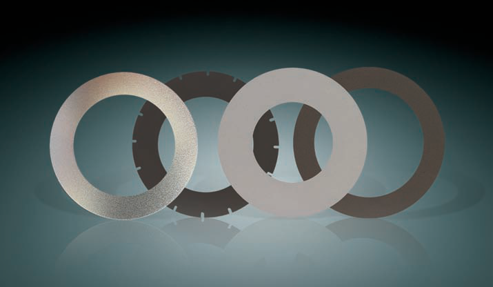
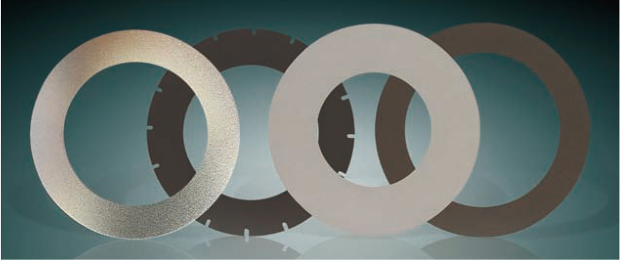
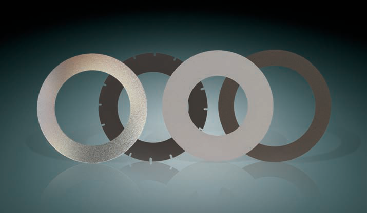
Metal- and resin-bonded microblades are designed for precise cutting with a narrow kerf. Free-cutting behaviour supports high spindle speeds and fast feeds. Blade development focuses on reduced chipping, cut quality and shape retention.
| Application group | Components and materials |
|---|---|
| Electronic packages | QFN, FBGA, CSP, MCP, POP, PBGA |
| Sawing and grooving | Ferrite, ceramic, glass, quartz and sapphire |
Minimum blade thicknesses
The three microblade product editions specify the same minimum thicknesses for the diameter groups below. Outer diameter, original inch designation and blade thickness are listed separately. The inch designations are size classes used in the product sheets, rather than exact conversions of the stated millimetre ranges.
| Outer Ø (mm) | Size class (inch) | Metal (mm) | Resin (mm) | Electroformed (mm) |
|---|---|---|---|---|
| 52–60 | 2.5 | 0.10 | 0.10 | 0.08 |
| 75–78 | 3 | 0.15 | 0.15 | — |
| 100–115 | 4 | 0.15 | 0.20 | — |
| 120–130 | 5 | 0.20 | 0.25 | — |
—: No minimum value is specified for electroformed blades in this diameter group.
Bond series: wear rate and relative hardness
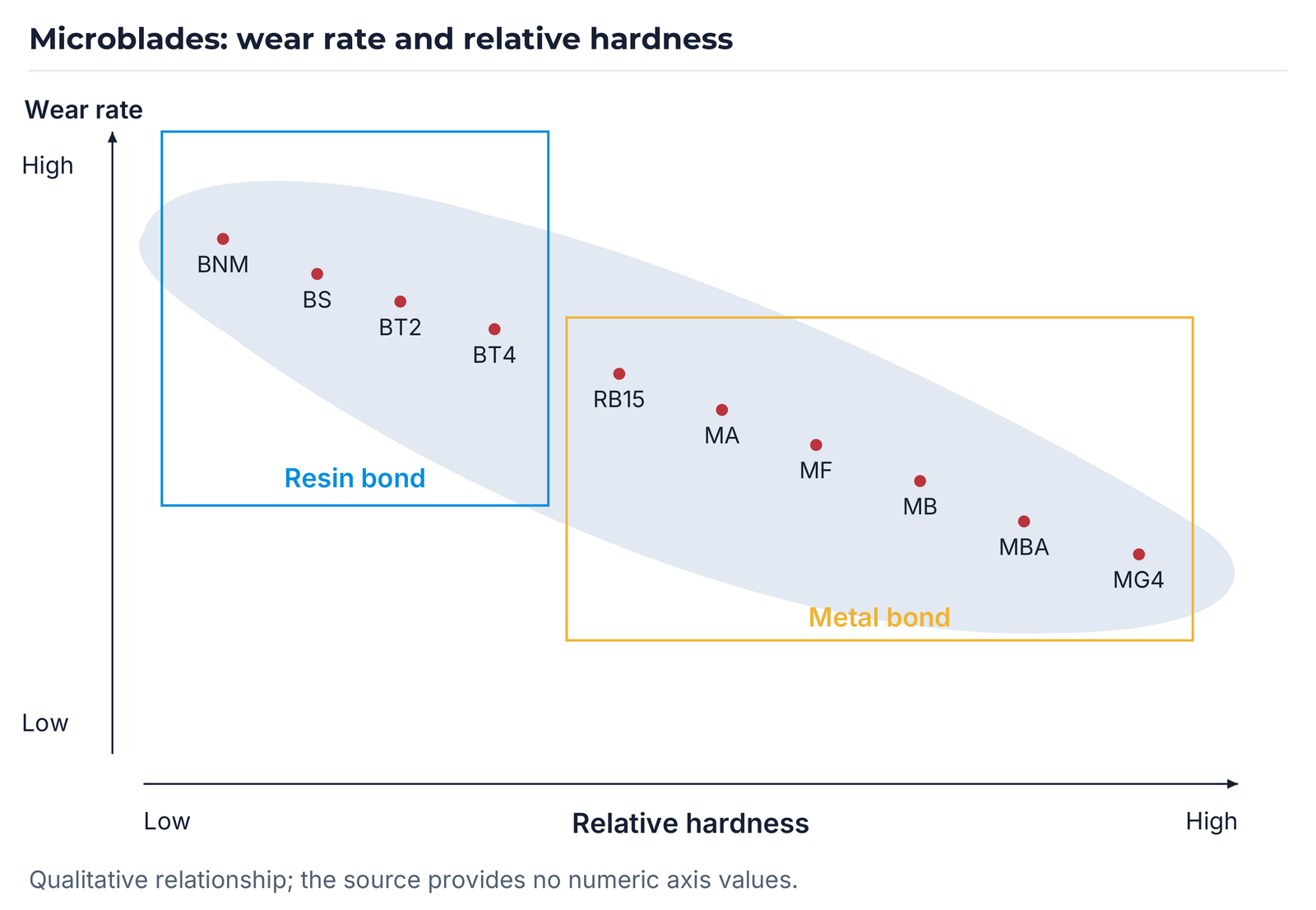
The qualitative relationship compares resin series BNM, BS, BT2 and BT4 with metal series RB15, MA, MF, MB, MBA and MG4. Relative hardness increases to the right; the illustrated wear rate ranges from low at the bottom to high at the top. The series lie within an overlapping range.

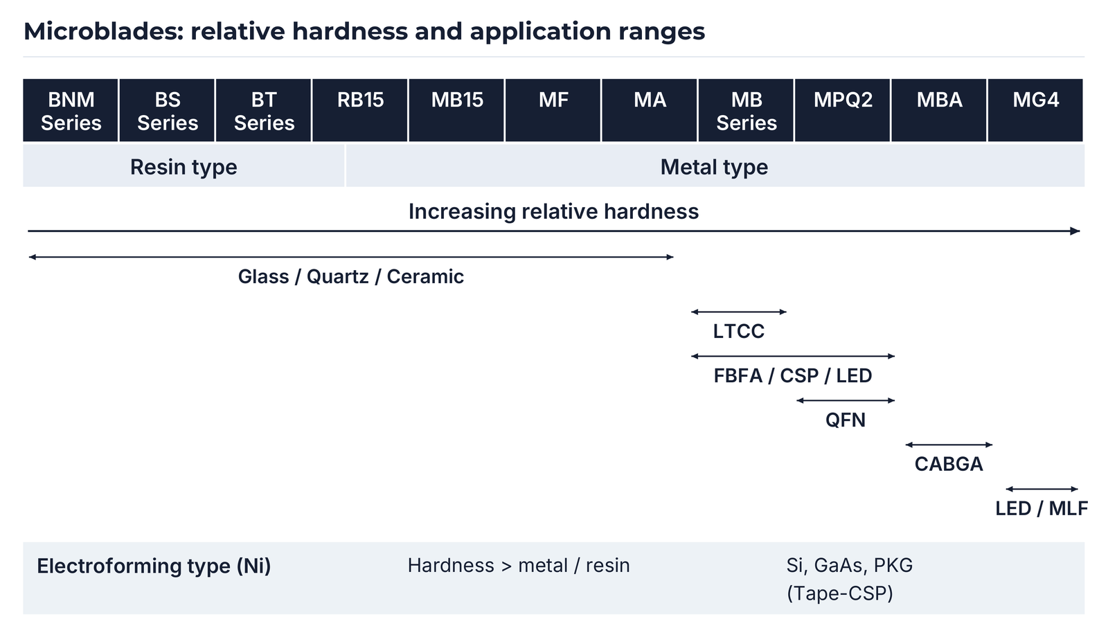
Blade structure and application ranges
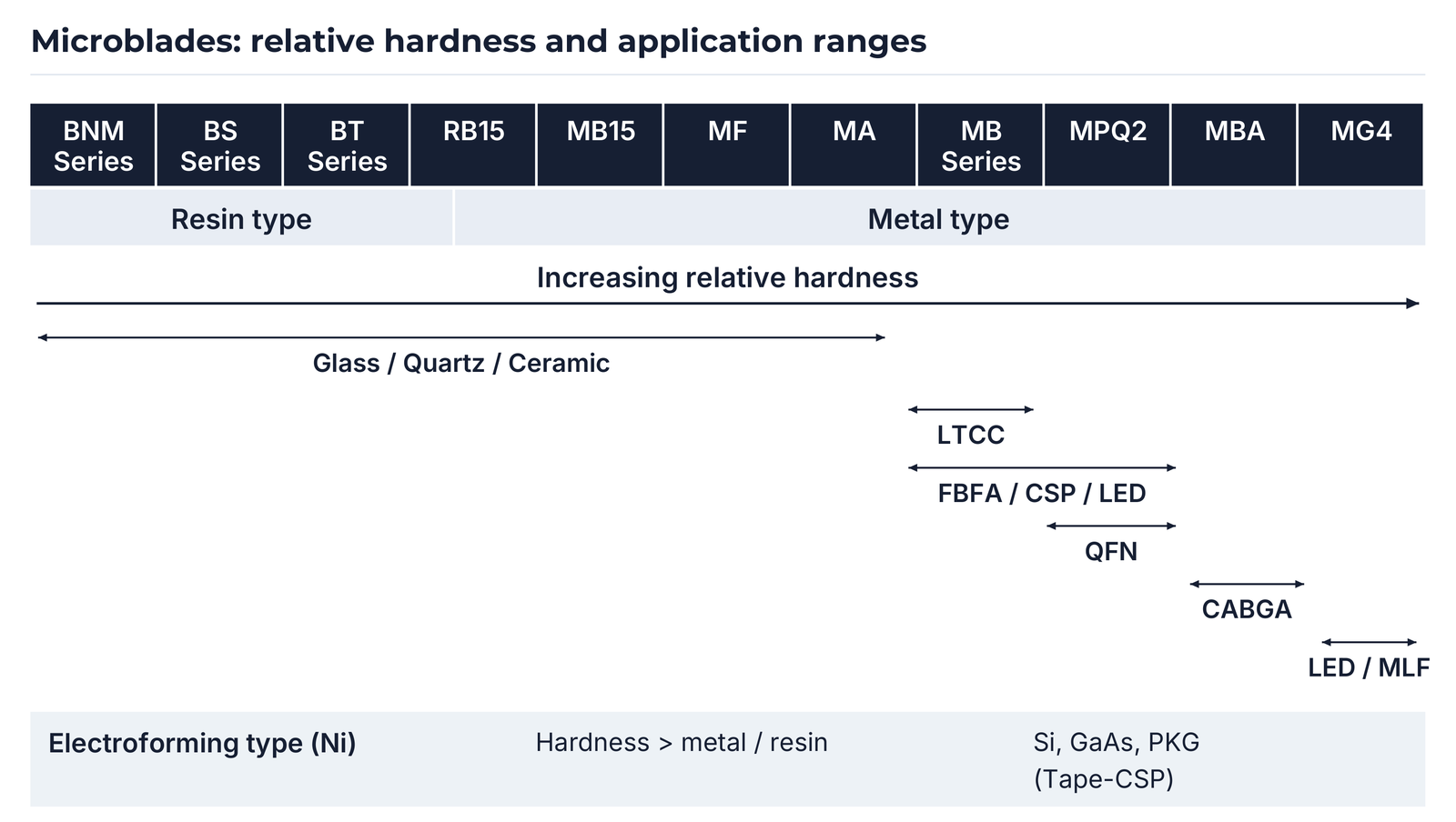
The selection matrix arranges BNM Series, BS Series, BT Series, RB15, MB15, MF, MA, MB Series, MPQ2, MBA and MG4 along increasing relative hardness. Application arrows indicate ranges within these series. The boundary between resin and metal lies within the RB15 column in the illustration, so the graphic should be read as a range relationship.
Application fields include glass, quartz and ceramic, LTCC, FBFA/CSP/LED, QFN, CABGA and LED/MLF. The electroformed structure uses metal (Ni); the matrix describes its hardness as higher than that of metal- and resin-bonded blades. Si, GaAs and PKG (Tape-CSP) cutting are listed as applications.
Blade surface and lateral diamond exposure
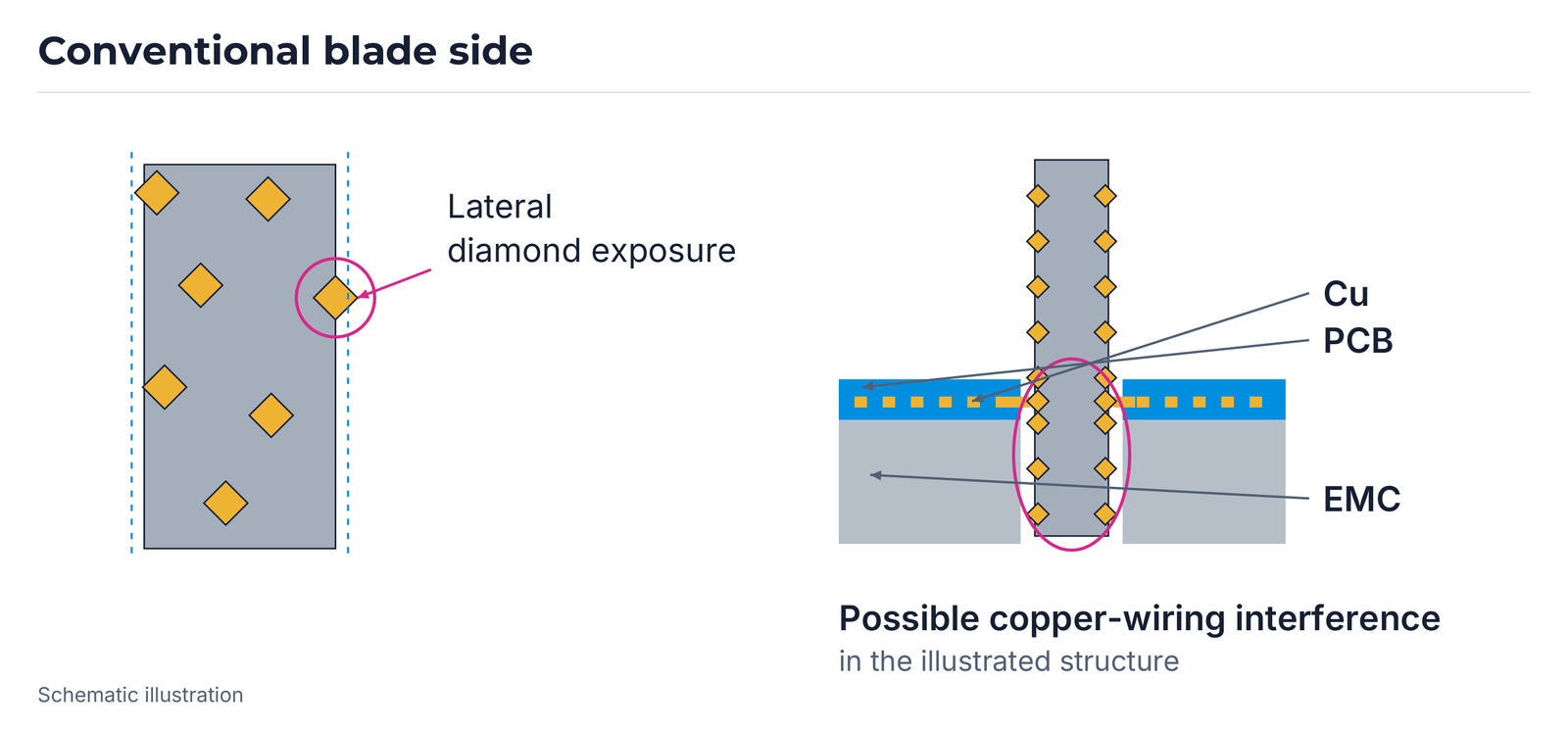
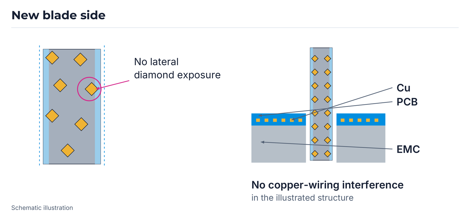
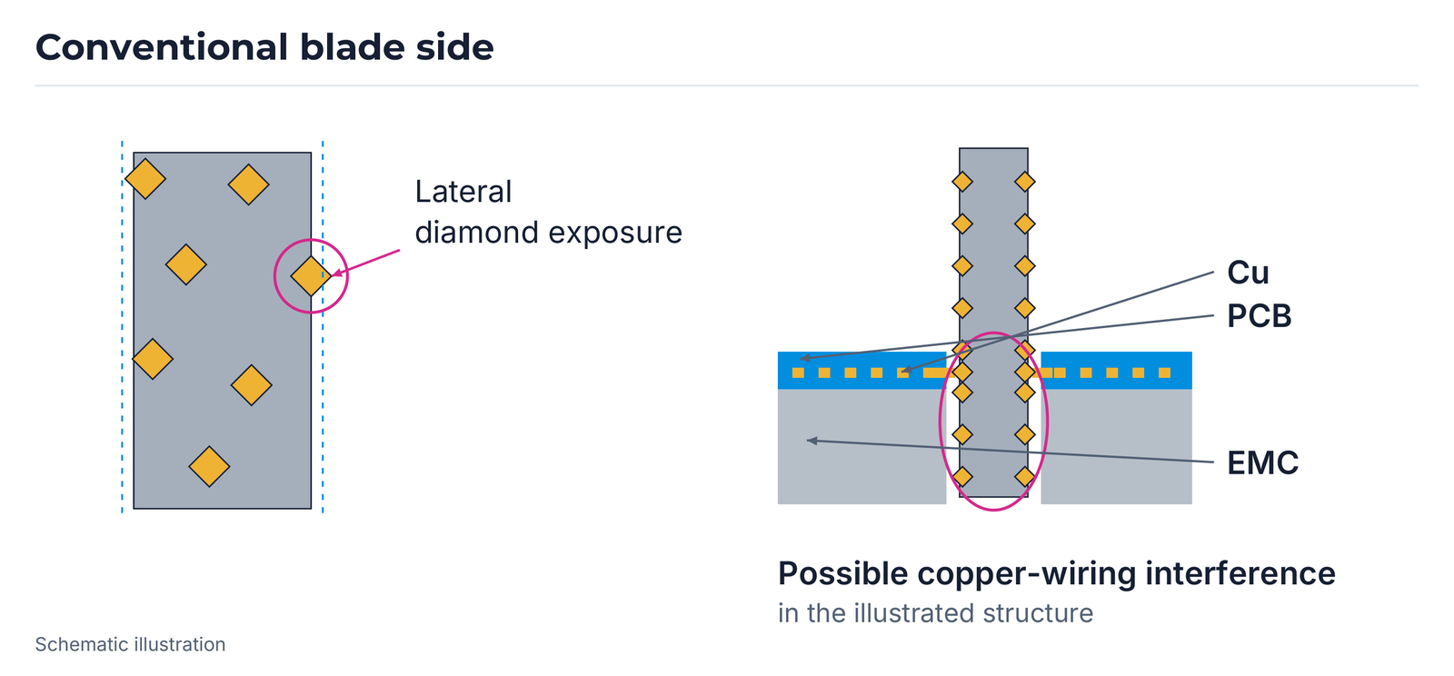
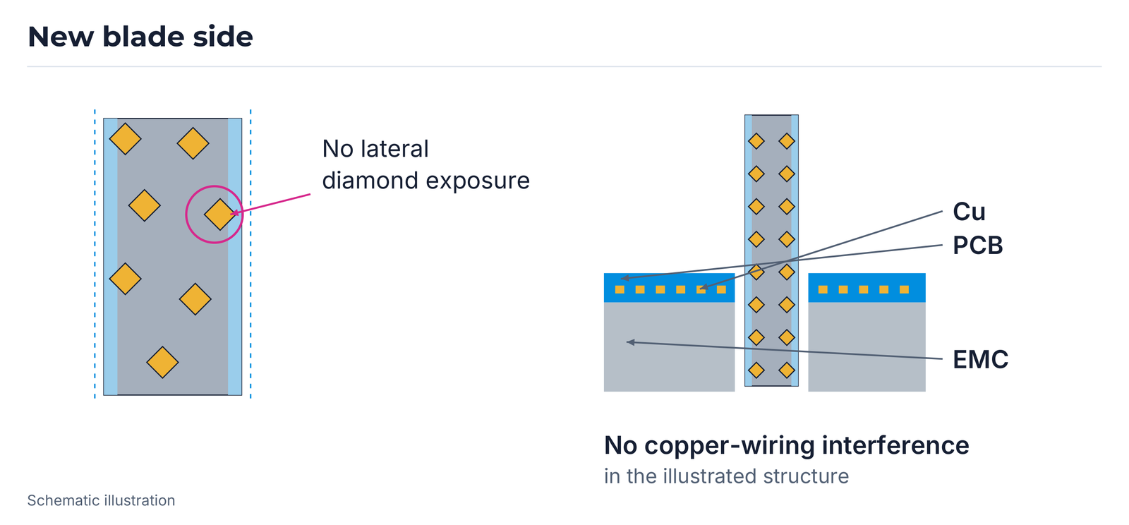
The new blade surface is designed so that diamonds do not protrude laterally beyond the blade face in the illustrated structure. The targets are better cut quality in terms of copper burrs and chipping, together with stable cut geometry. EHWA also describes longer blade life and greater hardness than the compared conventional design.
In the contact schematic, laterally exposed diamond can interfere with copper wiring in the PCB layer; the EMC layer lies below it. The new design avoids that contact in the illustrated structure. Cutting diamonds remain part of the tool.
Surface and shape comparisons
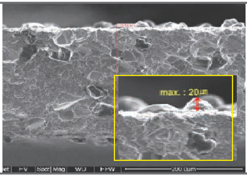
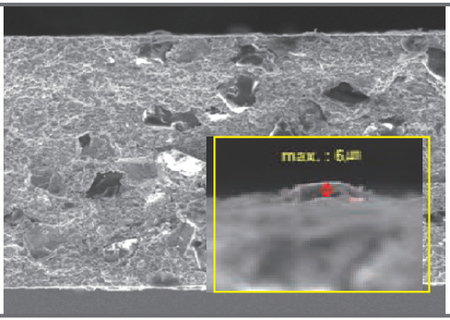
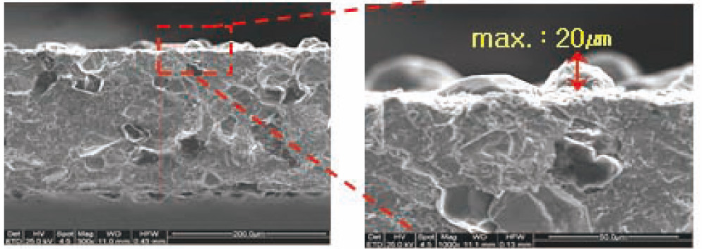
The SEM images show the conventional and new blade surfaces with an enlarged edge region. Micro-Blade 2018 and Micro-Blade 2018 New report a maximum of 20 µm for the conventional and 6 µm for the new design. Micro-Blade reports 20 µm and 3 µm in its separate image comparison. These image measurements belong to different product editions.
| Product edition | Conventional design | New design |
|---|---|---|
| Micro-Blade 2018 | max. 20 µm | max. 6 µm |
| Micro-Blade | max. 20 µm | max. 3 µm |
| Micro-Blade 2018 New | max. 20 µm | max. 6 µm |
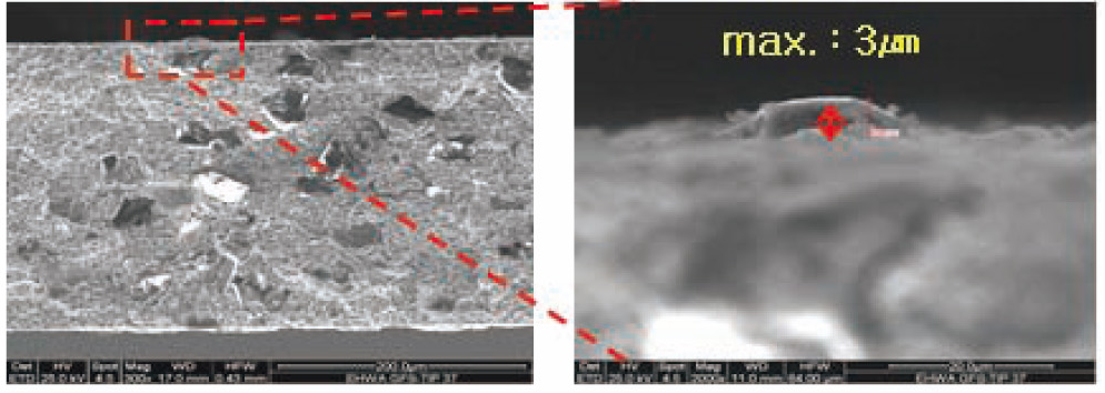

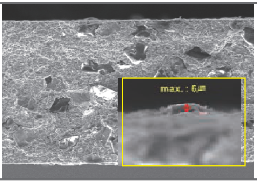
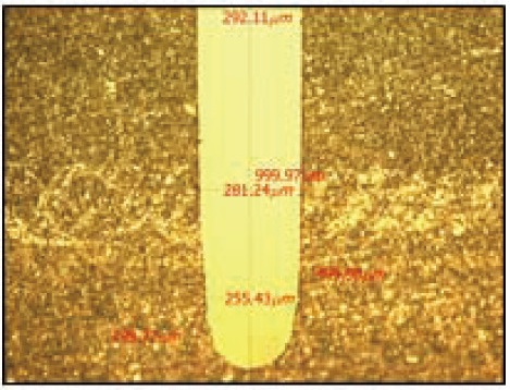
Micro-Blade supplements the surface comparison with optical images of the resulting groove. The original images retain all dimension lines and displayed measurements. Readable width values include 292.11, 281.24 and 255.43 µm in the conventional image, and 296.19, 298.03 and 281.24 µm in the image of the new design.

Package cut quality and blade comparison
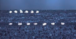
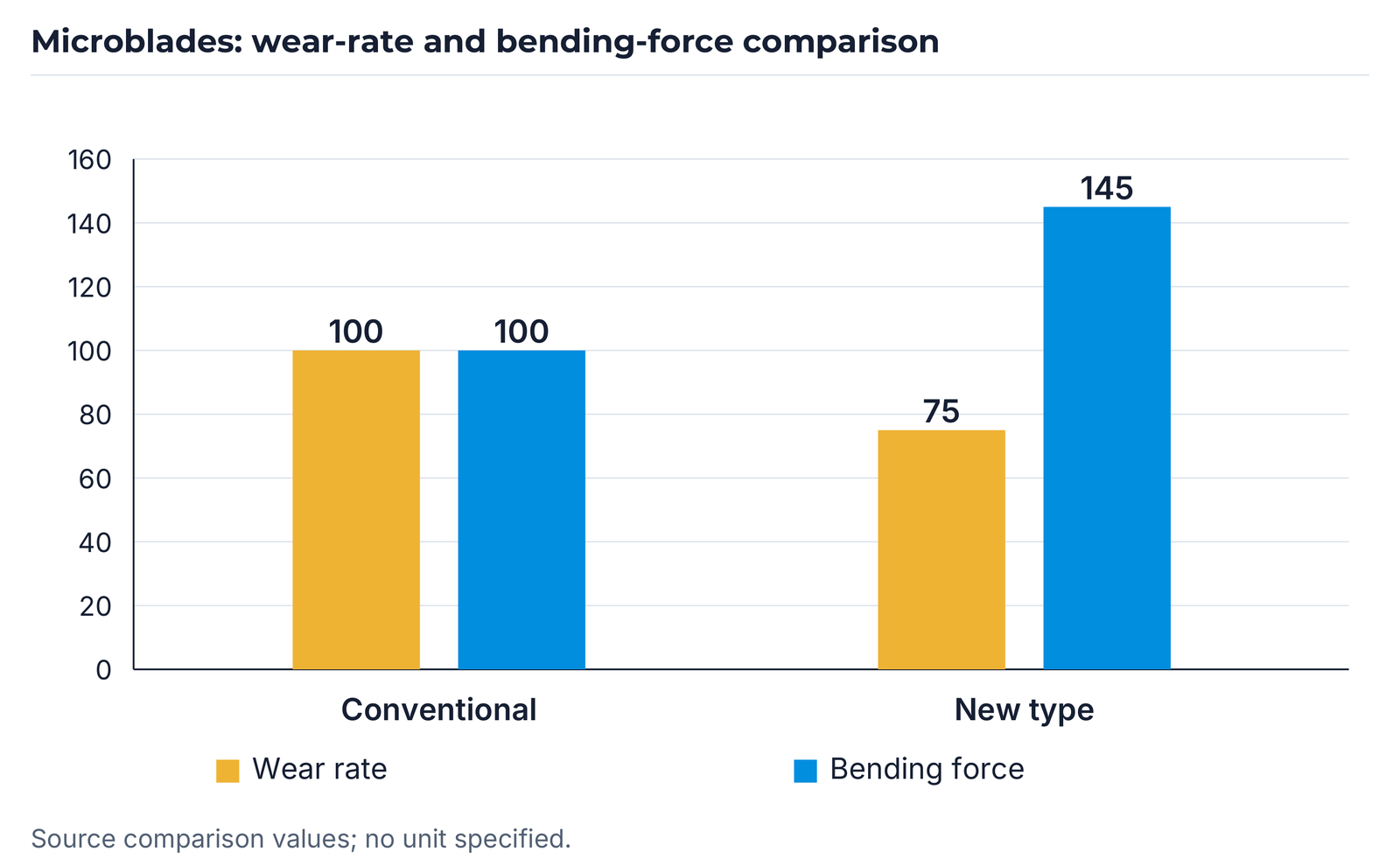
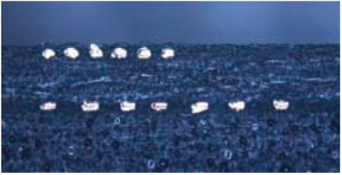
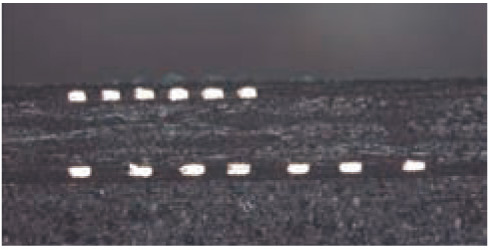
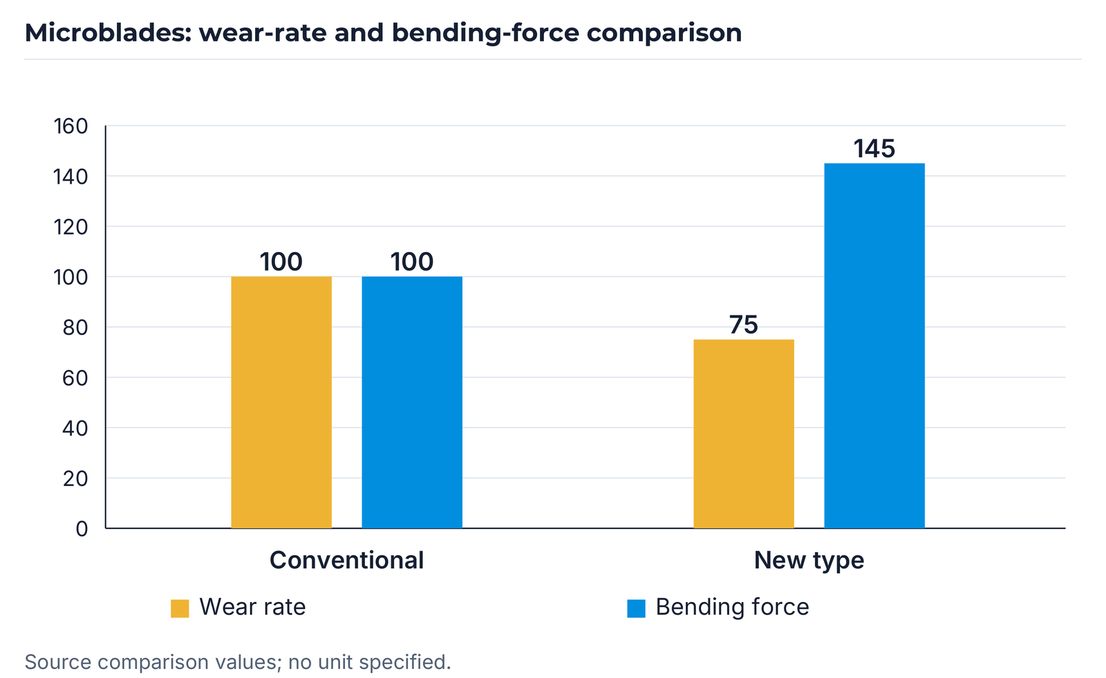
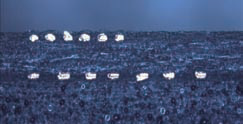
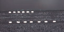
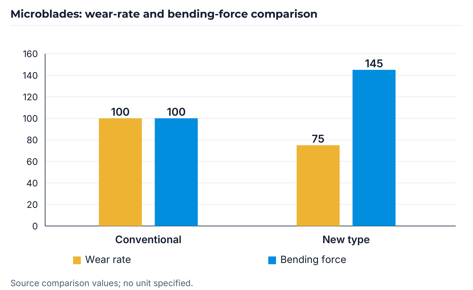
The package images compare conventional and improved cut quality. The associated blade comparison gives the following wear-rate and bending-force values. The sources provide no unit or complete trial conditions for these quantities; the numbers describe this comparison.
| Design | Wear rate | Bending force |
|---|---|---|
| Conventional | 100 | 100 |
| New type | 75 | 145 |
Electroformed microblades
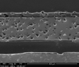
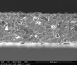
Electroformed nickel-bonded microblades combine high accuracy with a very thin, free-standing design. The product sheet describes a thickness of approximately 50 µm compared with more than 100 µm for metal-bonded microblades. Its specification also lists a blade thickness greater than 50 µm. The specific available design is determined for the application.
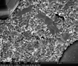
High bond retention strength supports long blade life. EHWA characterises the nickel-bond microstructure of this product development as pore-free. The design addresses hard materials, including ceramic LTCC and HTCC packages, and packages with a high abrasive content. High yield and long blade life are the described application benefits.
| Specification | Value |
|---|---|
| Blade thickness | >50 µm |
| Outer diameter | >54 mm |
| Diamond concentration | 25–100 con |
“con” is the concentration notation used in the product sheet; it is not identified as a percentage.
Electroformed microblades in package cutting
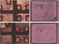
The applications combine a thin kerf with long blade life: ceramic HTCC and LTCC packages, LED packages, PCBs and other suitable components. The illustrated ceramic-package example reports chipping sizes of 10–20 µm with a maximum of 27 µm. Blade and machine parameters for this example are not specified.
Blade selection for your cut
For blade selection, we need the material and layer structure, component or wafer thickness, required kerf, top- and backside quality requirements, machine model, hub or flange interface, and spindle speed, feed and coolant conditions. For metal-containing packages, wiring structure, copper burrs and shape retention are particularly relevant. Existing cut images and blade-life data help compare suitable bond and grit variants.
Contact EHWA Europe: info@ehwadia.de · +49 6173 997780.
Product references
Product information is based on the complete EHWA editions Dicing (5.dicing), p. 1; Micro-Blade 2018, pp. 1–2; Micro-Blade, pp. 1–2; Dicing Blade, p. 1; Electroformed Micro Blade New, pp. 1–2; Micro-Blade 2018 New, pp. 1–2; and Dicing Blade New, p. 1. Matching minimum thicknesses and comparison values are consolidated; differing measurement images and all image variants remain attributed.
The context for backside chipping additionally considers DISCO: Dicing of thin wafers. The editorial date identifies the preparation of this edition, rather than the manufacturing year of the blades.