Dicing, back grinding, CMP conditioning and wafer-edge grinding
Tools matched to the process chain
EHWA combines precision cutting, back grinding and edge grinding with CMP pad conditioning. Different blade structures, bonds and tool forms support processing of silicon, compound semiconductors, sapphire, SiC, glass and other hard materials. Selection considers the workpiece, machine, mounting, process conditions and required quality.
Microblades: thin blades and efficient cutting
The precision thin blades are designed for high cutting efficiency. Their free-cutting action supports suitable high spindle speeds and feed rates. The blade structure helps reduce chipping during sawing and achieve consistent cut quality.

| Order | EHWA series |
|---|---|
| 1 | BNM Series |
| 2 | BS Series |
| 3 | BT Series |
| 4 | RB 15 |
| 5 | MB 15 |
| 6 | MF |
| 7 | MA |
| 8 | MB Series |
| 9 | MPQ2 |
| 10 | MBA |
| 11 | MG4 |
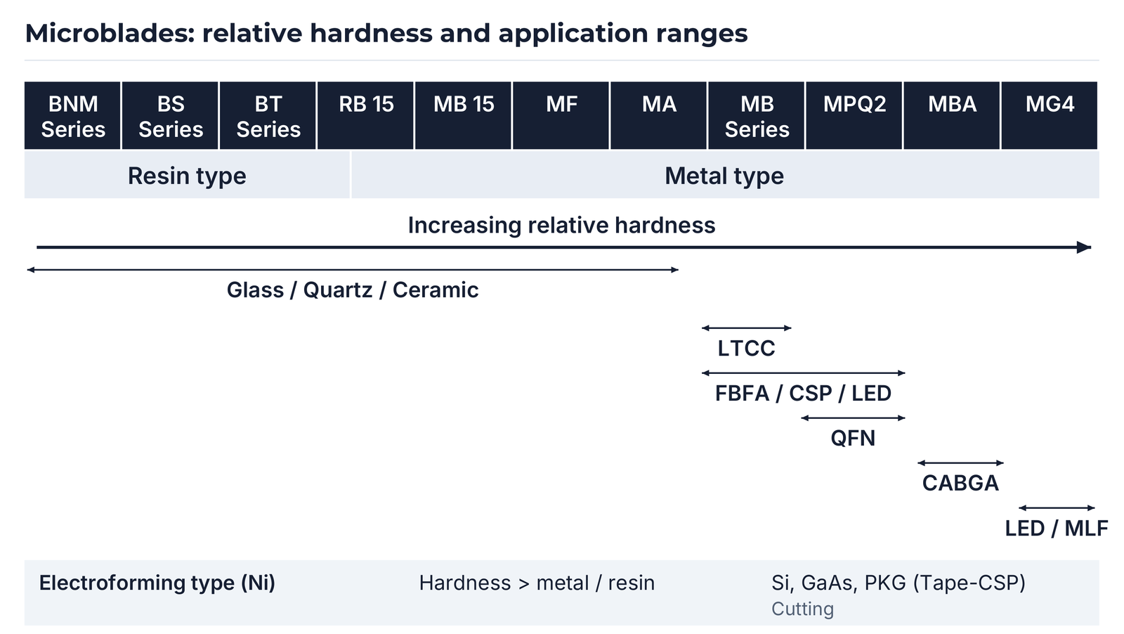
The range shows resin and metal bonds with increasing relative hardness. The bond transition lies within the RB 15 column. Range arrows identify glass/quartz/ceramic, LTCC, FBFA/CSP/LED, QFN, CABGA and LED/MLF. They indicate application ranges within the programme rather than a numerical hardness scale.
The separate electroforming structure identifies nickel as the metal bond and higher relative hardness than metal/resin types. Listed applications are Si, GaAs and PKG (Tape-CSP).
Side enhancement for the PCB/EMC structure
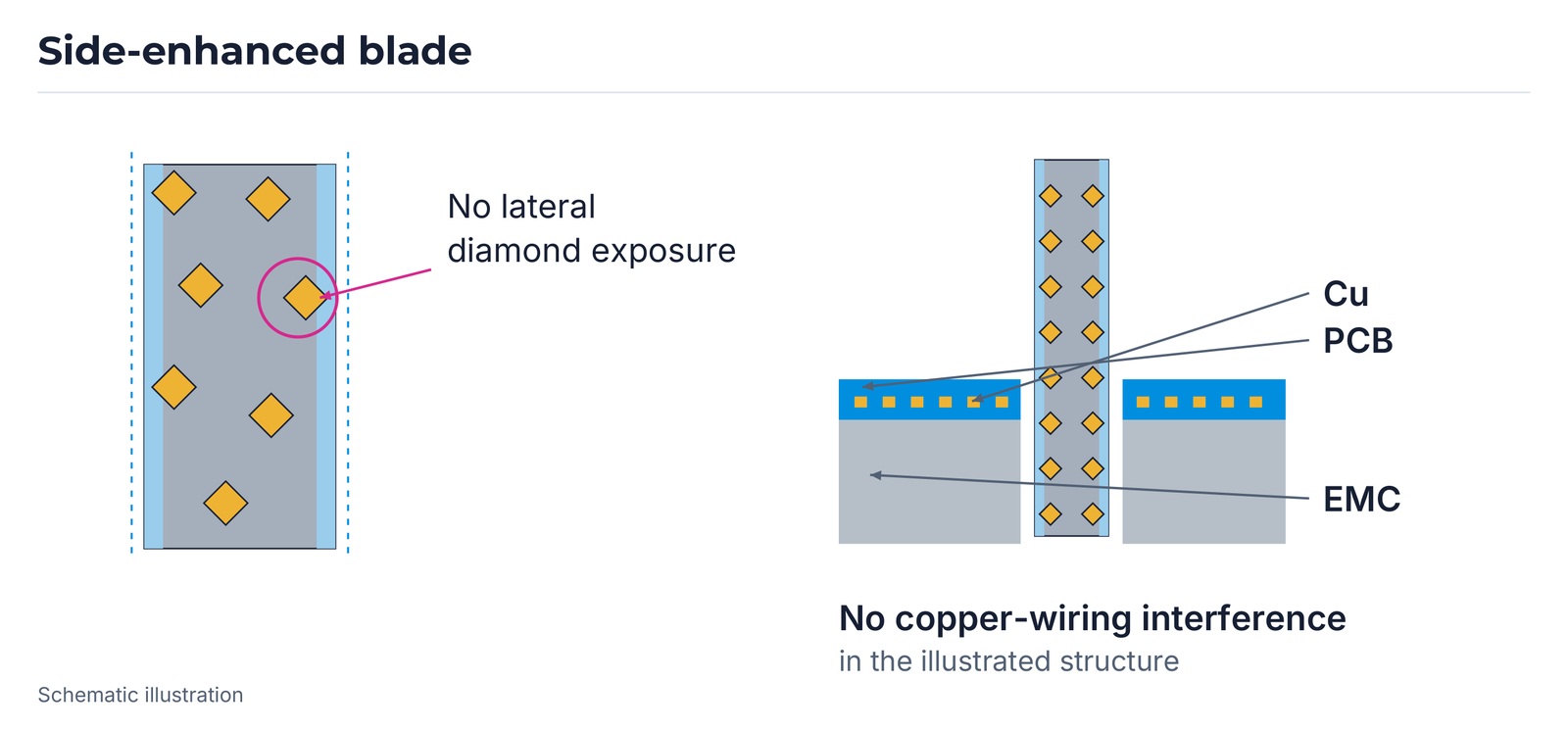
Laterally exposed diamonds on a conventional blade can contact copper wiring within the PCB. Side enhancement keeps the diamonds laterally within the blade contour in the illustrated structure and avoids the depicted copper-wiring contact. The cut schematic separately identifies PCB, Cu and the underlying EMC mould compound.

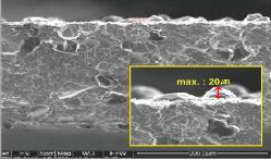
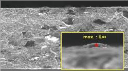
| Blade side | Local detail marking |
|---|---|
| Conventional | maximum 20 µm |
| Side-enhanced | maximum 6 µm |
The markings refer to the illustrated SEM details, not the overall blade thickness.
Dicing blades: precision and consistent quality
EHWA develops very thin, accurate dicing blades. Controlled diamond-particle and grit-size distribution supports low chipping and consistent cut quality. Suitable high feed rates improve productivity; the tool is designed for the customer's application.
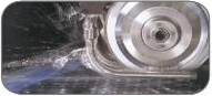

Position 1 identifies the wafer top side and position 2 the back side. Fine diamond grit supports low top-side chipping. Coarser grit can support back-side quality through cutting ability and lower load per grain. Grit, feed rate, cut depth and coolant delivery are selected as a combined process. In conventional blade dicing, cutting water cools the processing point and removes cutting particles.
Bond development for Si and compound semiconductors
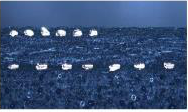
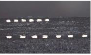
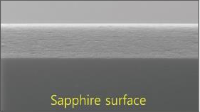
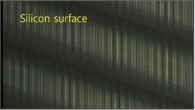
Bond development targets silicon and compound semiconductors. Low top- and back-side chipping and suitable high feed rates combine cut quality with productivity. The images show the top surface and the side/back view of the application example.

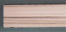
Back grinding: resin and metal range
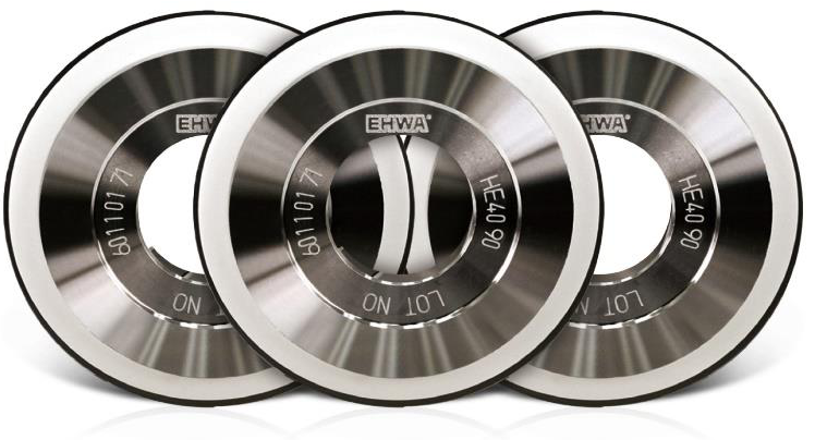
The wheels are designed for different machines and applications, including simultaneous grinding of multiple wafers. Their design combines long tool use with high bulk removal. Matched wheel designs and process recipes support different grinding methods.
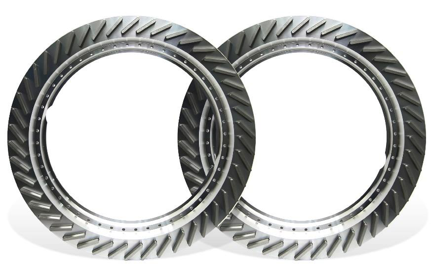
Applications include silicon wafers, sapphire wafers, SiC wafers, glass wafers and high-hardness materials such as zirconia.
| Process | Series designation | D [mm] | W [mm] | X [mm] | Grit |
|---|---|---|---|---|---|
| Rough | RS, MS Series | 200–380 | 2–5 | 3–10 | #170–#800 |
| Fine | SW Series | 200–380 | 2–5 | 3–10 | #1200–#4000 |
CMP conditioning: strong mechanical and chemical diamond retention
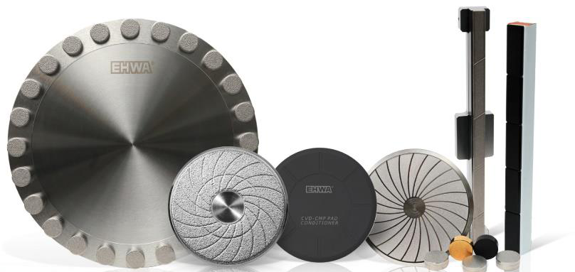
EHWA uses proprietary brazing powders and high-temperature/vacuum brazing processes. Combined mechanical and chemical bonding provides strong diamond retention in CMP conditioning disks. The range includes disk and bar forms.
| Comparison image | Usage duration | Observation |
|---|---|---|
| Electroplated disk | 20 h | Heavy diamond loss observed |
| EHWA BSL disk | 60 h | No diamond loss observed |
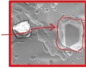


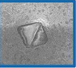
The images document different usage durations; other comparison conditions are not specified.
CVD conditioners: tip geometry and process performance
Proprietary brazing and diamond-orientation technology supports high pad cut rate (PCR) maintained during use. For CVD conditioners, EHWA describes very small (“near-zero”) deviations in diamond-tip height to reduce wafer defects and unwanted topography.
Customised tip configurations allow PCR, pad surface roughness and wafer material removal rate (MRR) to be adjusted. Low diamond wear supports use across multiple pads and can lower cost of consumable (CoC) per wafer. For SiC CMP, EHWA identifies CVD conditioners as a technology for high MRR and as a process of record (POR); design is matched to the specific SiC process.
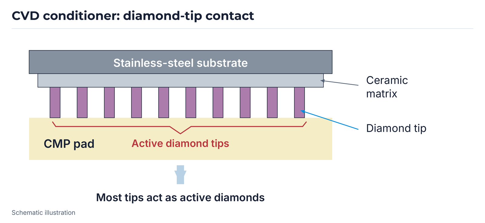
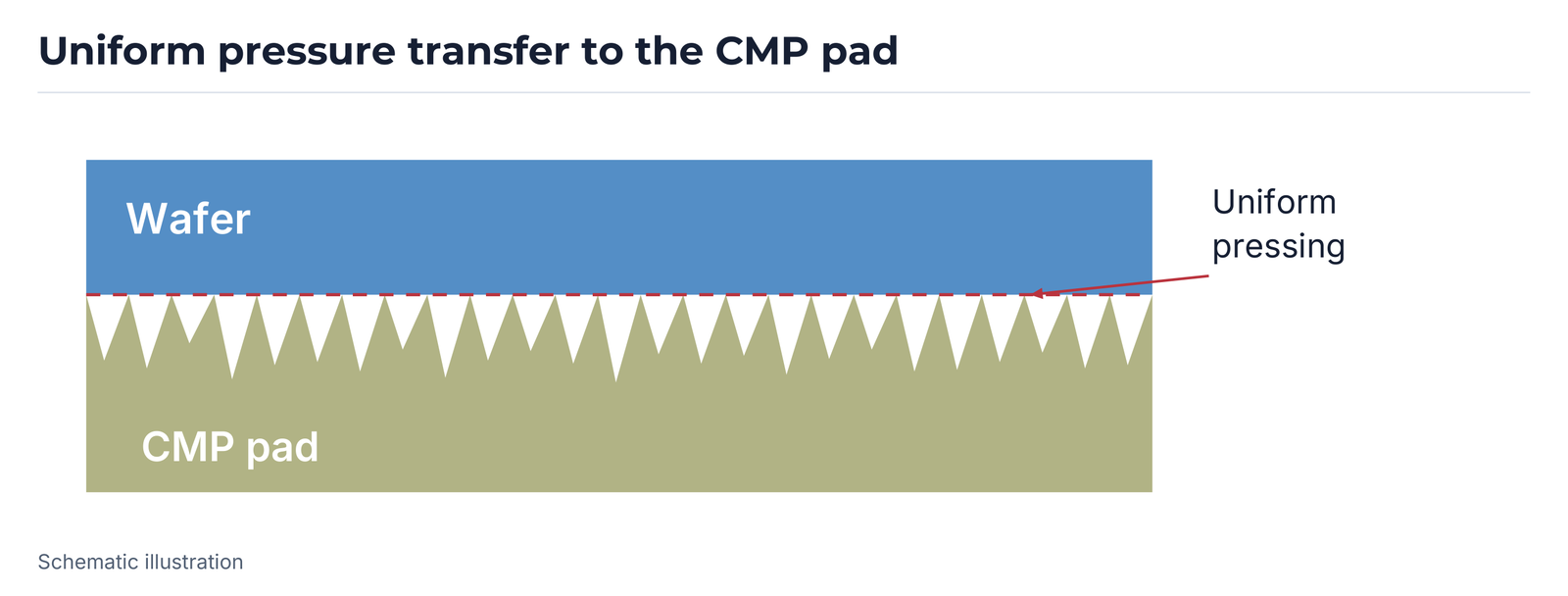
Most tips act as active diamonds in the illustrated contact model. Uniform tip height supports uniform pressure transfer to the structured pad surface.
Pad use over eight cycles

| Pad cycle | Diamond disk: relative pad wear rate ratio | CVD disk: relative pad wear rate ratio |
|---|---|---|
| 1 | 100 % | 72 % |
| 2 | 76 % | 69 % |
| 3 | no value shown | 79 % |
| 4 | no value shown | 82 % |
| 5 | no value shown | 75 % |
| 6 | no value shown | 80 % |
| 7 | no value shown | 77 % |
| 8 | no value shown | 78 % |
The example shows two pads per diamond disk and eight pads per CVD disk. Percentages describe relative pad wear rate ratio. Pad life and replacement intervals are matched to the CMP process.
Edge tools for silicon and sapphire wafers
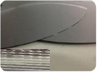
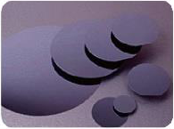
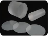
Different groove profiles allow tool design for different wafer edges. High tool rigidity supports uniform chamfer widths. Strong profile retention and tool versions for multiple rough/fine grinding stages combine form quality with process performance.
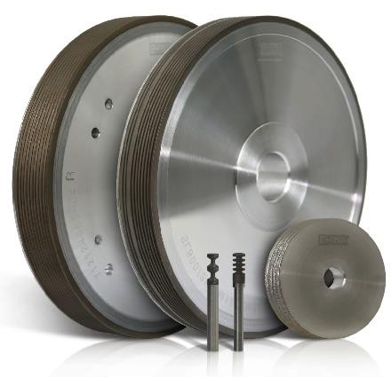
| Type | Diameter designation | Groove (1) | Thickness [mm] | Grit | Groove (2) |
|---|---|---|---|---|---|
| MD-DW | Ø3.9 | 5G | 5–20 | #325–#3000 | 5G |
| MD-1FF6Y | Ø202 | 8G | 5–20 | #325–#3000 | 8G |
No unit is given for the diameter designations. Both groove columns carry matching identifiers; diameter and groove geometry are confirmed during tool selection.
Measurement references for the edge profile
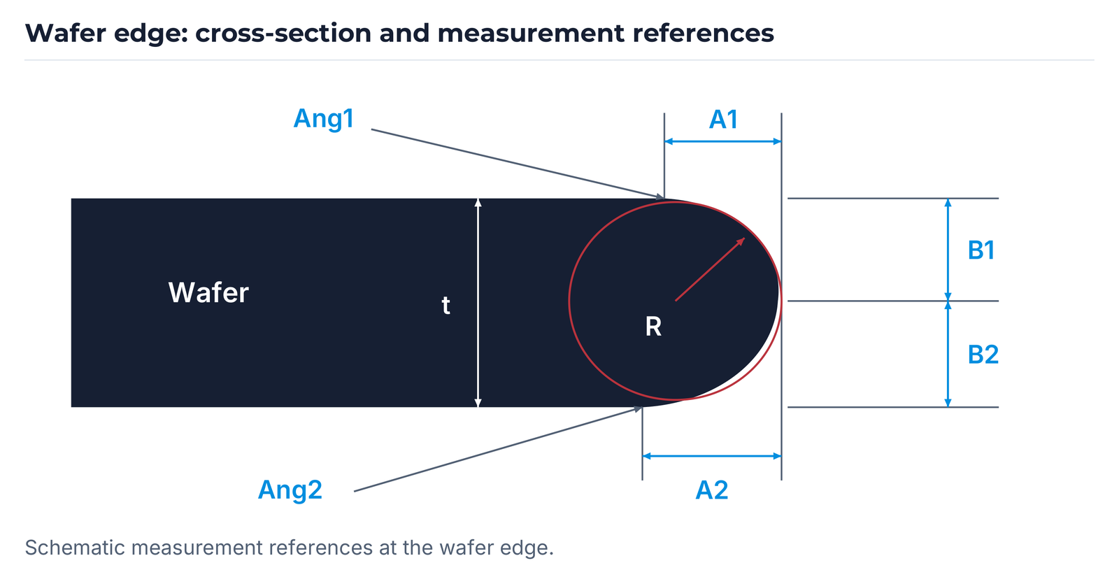
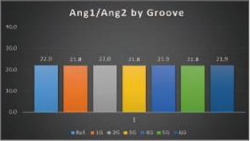
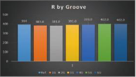
A1 and A2 identify upper and lower horizontal profile references; B1 and B2 identify vertical distances to the middle reference. Ang1 and Ang2 mark upper and lower angle references, R the radius and t the wafer thickness. Numerical dimensions follow the agreed edge form.
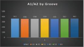
The three measurement plots compare A1/A2, Ang1/Ang2 and R by groove. Colour series identify Ref. and 1G through 6G. Measurement examples support matching the groove profile to the required edge form.
| Plot title | Measurement reference |
|---|---|
| A1/A2 by Groove | Upper/lower horizontal profile reference by groove |
| Ang1/Ang2 by Groove | Upper/lower angle reference by groove |
| R by Groove | Radius comparison by groove |
Discuss your semiconductor application
Provide the workpiece material, wafer/package dimensions, machine, mounting and current tool specification. For cutting and grinding, useful details include feed rate, spindle speed, coolant delivery and target chipping, surface and edge form. For CMP, add the pad, slurry, PCR, wafer removal and replacement intervals. Existing information is enough to start the discussion.
EHWA Europe: info@ehwadia.de · +49 6173 997780
Technical source
EHWA, Semiconductor Product Range, five pages. Editorial edition: 13 October 2026.