Back-grinding wheels, microblades, dicing blades and CMP pad conditioners
EHWA DIAMOND – since 1975
Design the tool and process together
This programme combines material removal during back grinding, wafer and package singulation, and CMP pad conditioning. EHWA provides different bonds, cutting structures and tool forms for these operations. The material, machine, cutting or grinding conditions and required surface determine the selection.
Back grinding with resin and metal bonds
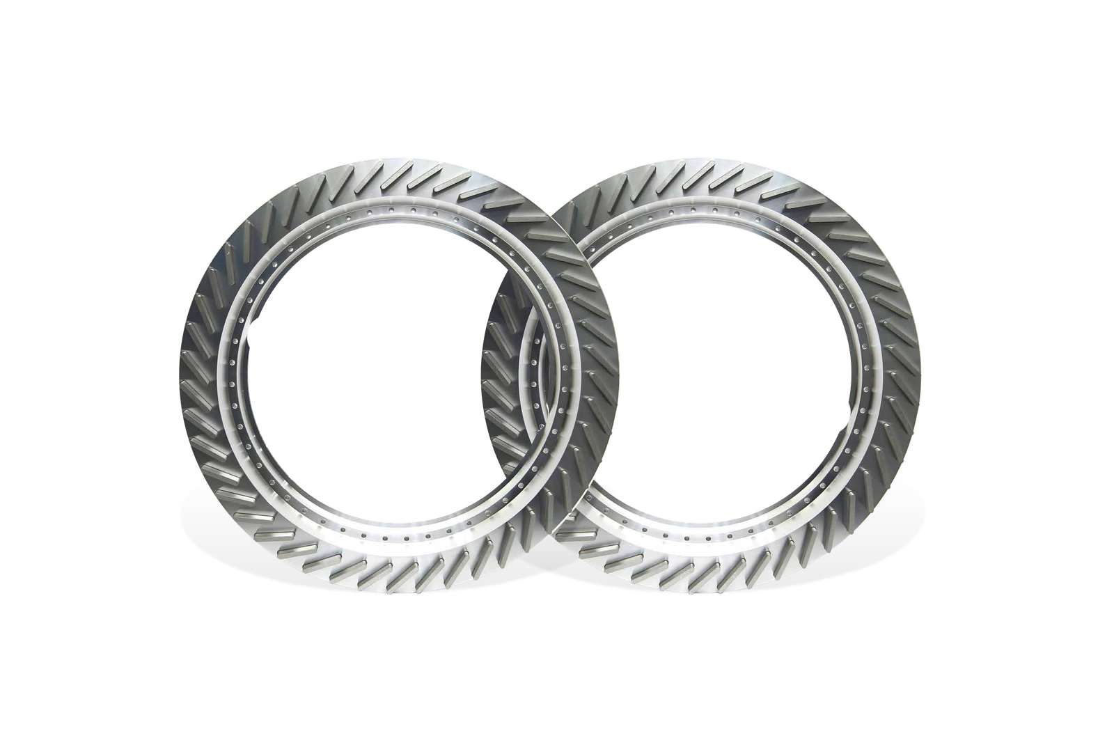
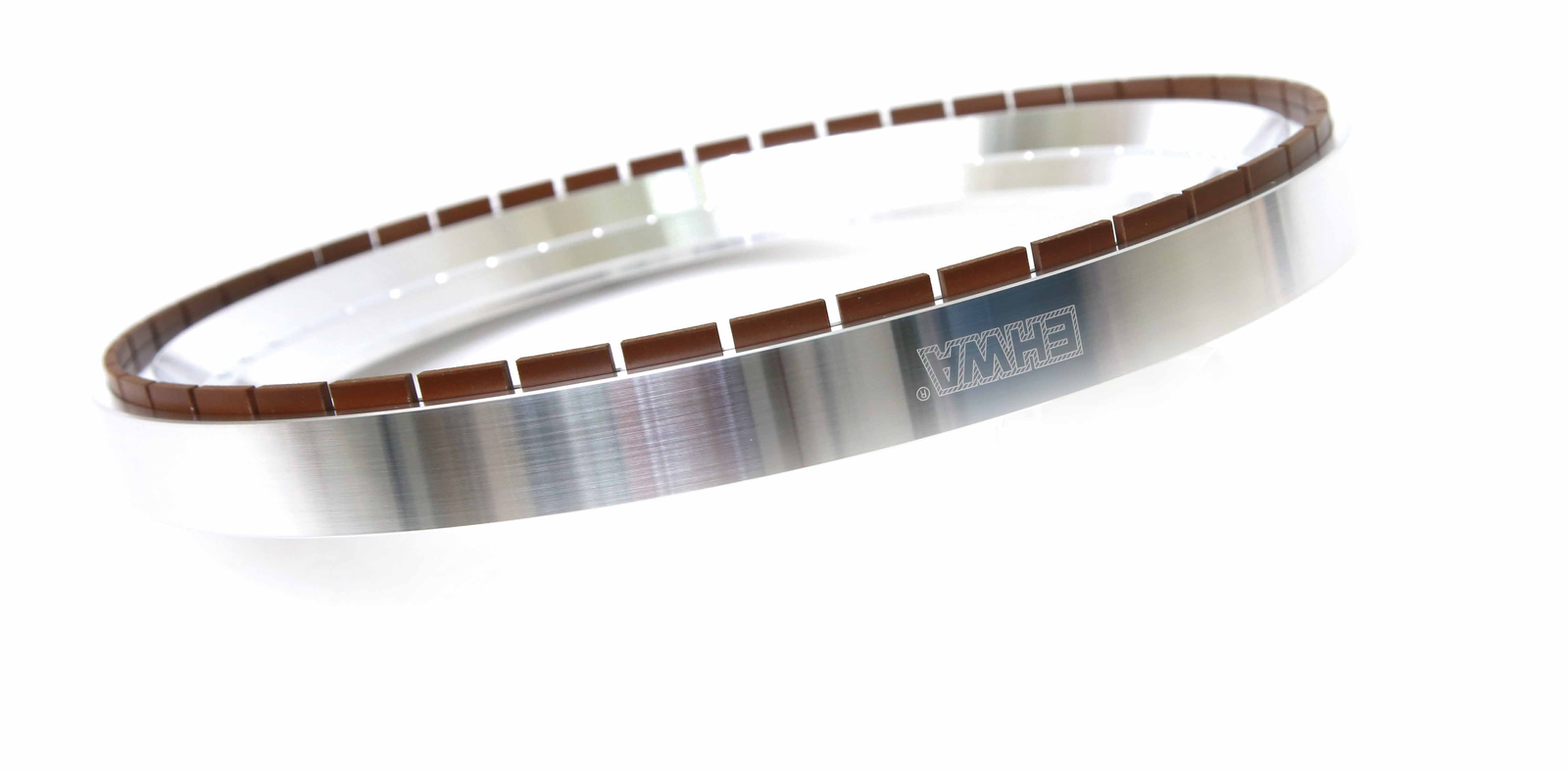
The EHWA programme covers different machine types, applications and grinding methods, including designs for grinding several wafers simultaneously. It is designed for long wheel life and high bulk removal rates. Wheel construction and process parameters are matched to the machine and grinding method.
Listed applications are silicon wafers, sapphire wafers, silicon carbide wafers, glass wafers and high-hardness materials such as zirconia. The document distinguishes rough and fine grinding:
| Process | Bond series | D (mm) | W (mm) | X (mm) | Grit designation |
|---|---|---|---|---|---|
| Rough grinding | RS, MS Series | 200–380 | 2–5 | 3–10 | #170–#800 |
| Fine grinding | SW Series | 200–380 | 2–5 | 3–10 | #1200–#4000 |
D, W and X are the dimensional labels in the EHWA specification. Their definitions, wheel mounting and processing sequence are agreed during tool selection.
Microblades: bond programme and cutting performance
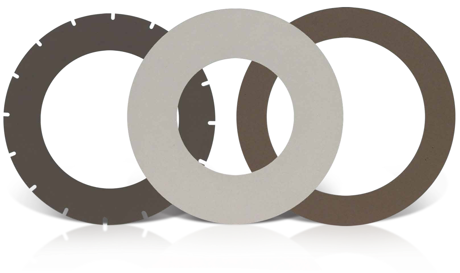
The thin precision blades are designed for efficient cutting. EHWA describes free-cutting action at high rotational speeds and fast feed rates, together with reduced chipping during sawing. Cutting quality, feed rate and tool wear are matched to the actual material structure.
The selection matrix presents the following series in the direction of increasing relative hardness:
| Position in the selection matrix | EHWA designation |
|---|---|
| 1 | BNM Series |
| 2 | BS Series |
| 3 | BT Series |
| 4 | RB 15 |
| 5 | MB 15 |
| 6 | MF |
| 7 | MA |
| 8 | MB Series |
| 9 | MPQ2 |
| 10 | MBA |
| 11 | MG4 |
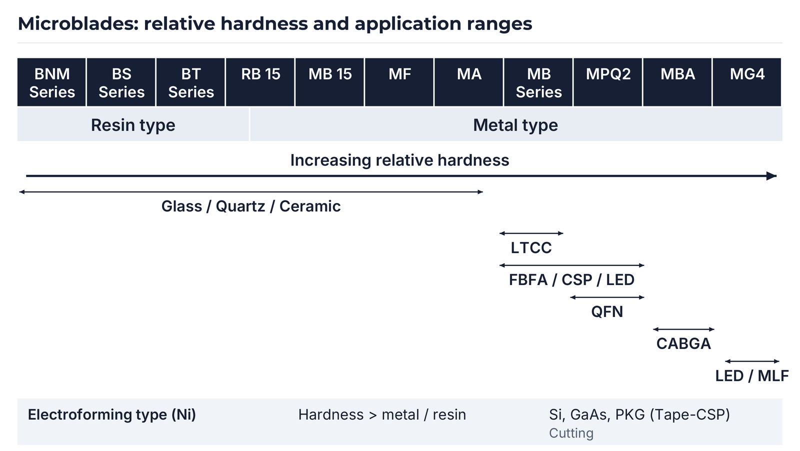
The matrix shows application ranges for glass, quartz and ceramics, as well as LTCC, FBFA/CSP/LED, QFN, CABGA and LED/MLF. The range arrows support series selection according to the material and package structure. The resin/metal boundary runs within the RB 15 column; the specific bond design is matched to the application.
Electroformed designs with a nickel bond (Electroforming Type) form a separate group. In this qualitative selection, EHWA places their hardness above the illustrated metal/resin types and lists cutting Si, GaAs and Tape-CSP packages.
Side enhancement: control contact with copper structures
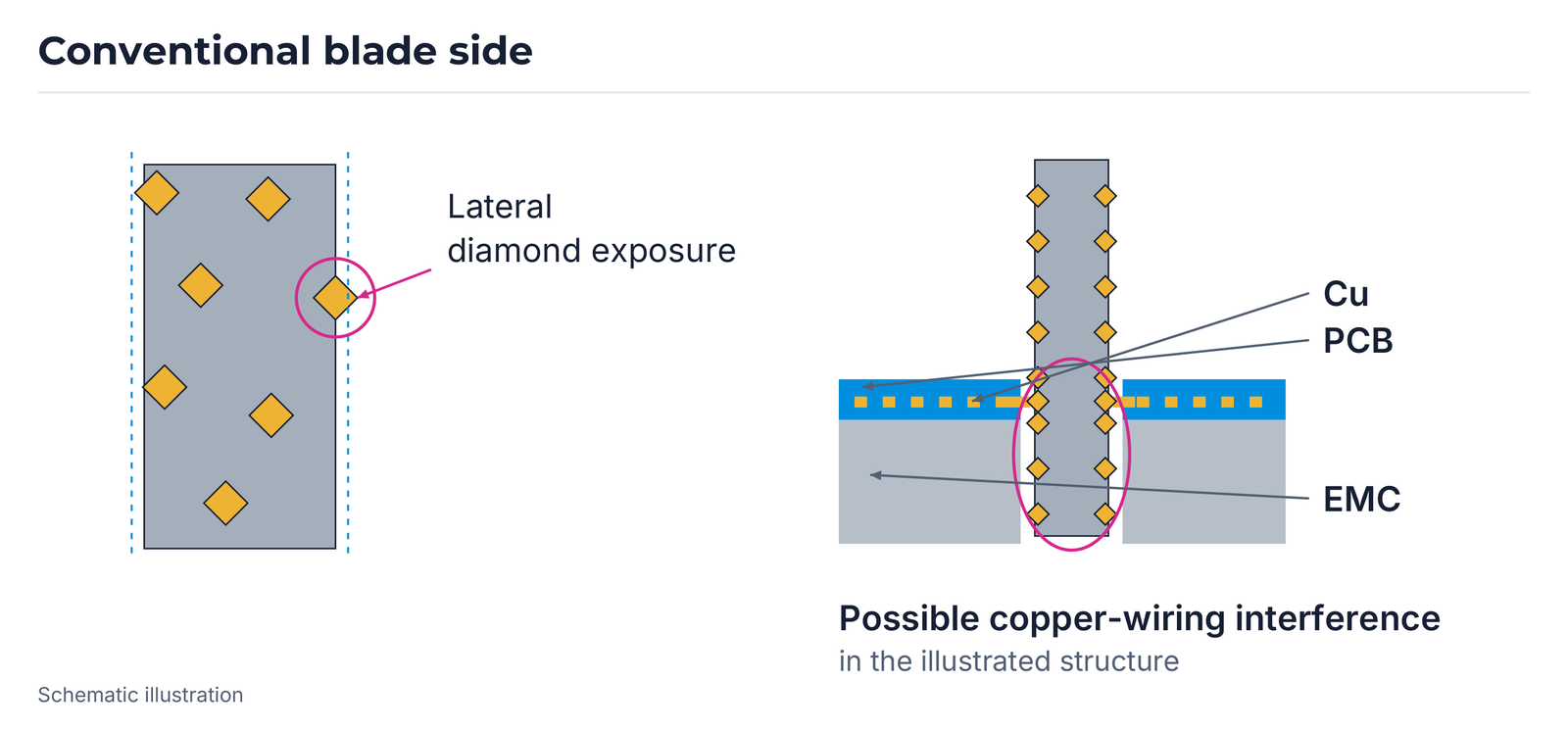
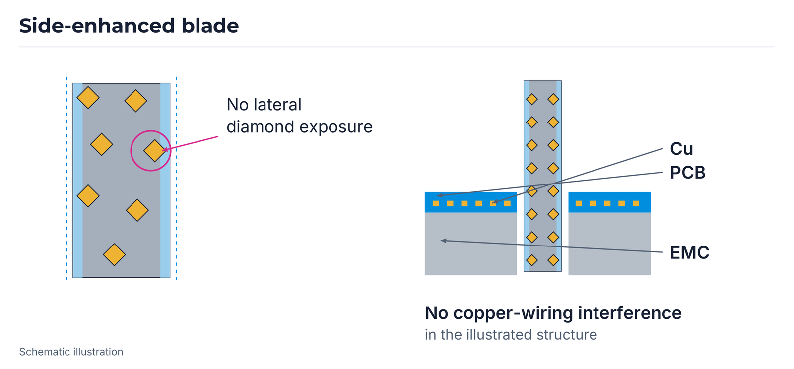
The structure comparison distinguishes a conventional blade side from a side-enhanced design. Diamonds protruding from the blade side can contact copper wiring in the illustrated PCB/EMC structure. The enhanced side avoids this lateral contact in the example shown.
| Image example | Marking in the detailed image | Statement illustrated by the structure diagram |
|---|---|---|
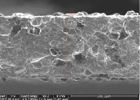
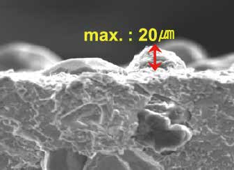
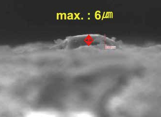
| Conventional side | maximum 20 µm | Side diamond exposure; possible interference with copper wiring |
| Side-enhanced design | maximum 6 µm | No side diamond exposure in the illustrated example; no contact with copper wiring |
The 20/6 µm values belong to the marked local surface details. They do not describe the overall thickness of every microblade.
Dicing blades: thin cuts and controlled chipping
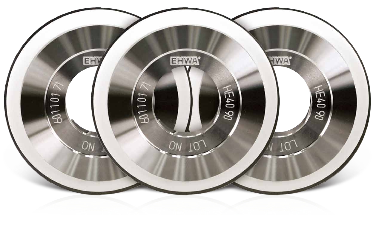
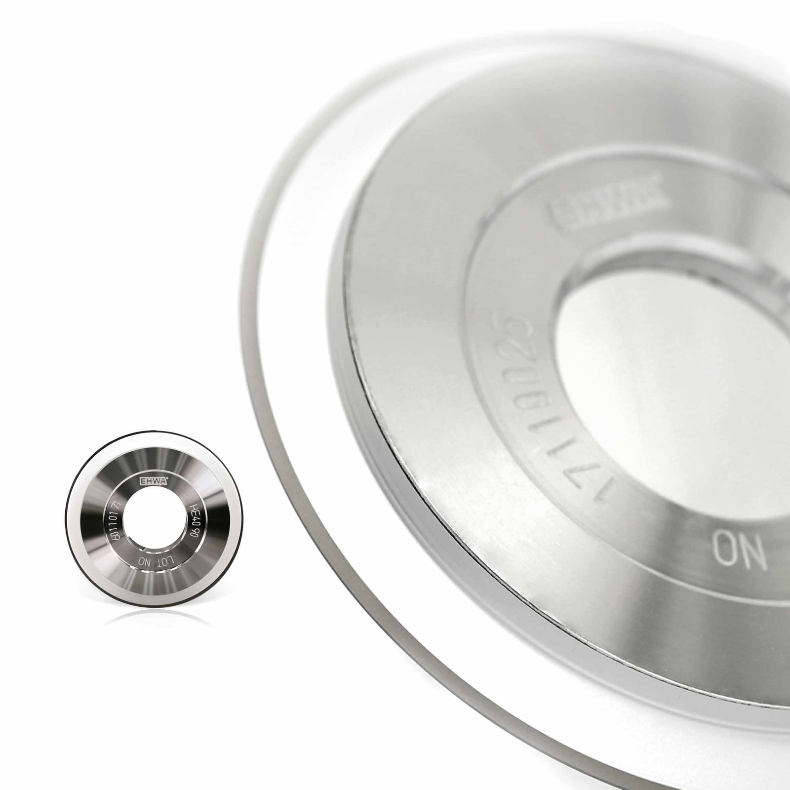
EHWA offers particularly thin, accurate dicing blades. Controlled diamond particle and grit-size distribution supports low chipping and consistent cutting quality. Suitable high feed rates can improve productivity. The tool and process are designed for the customer's application.
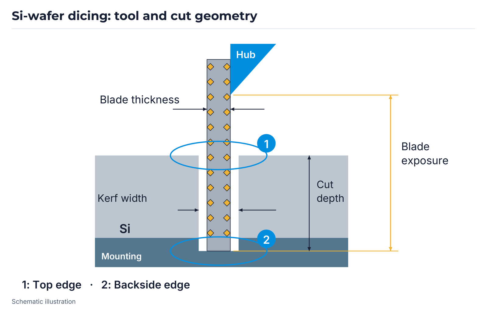
The diagram distinguishes the top edge (position 1) from the backside edge (position 2). Finer diamond grits are associated with small top-side chips. Coarser grits can influence backside cutting quality through their cutting ability and reduced loading on individual grains. These relationships are considered together with blade thickness, exposure, kerf width, cut depth and mounting.
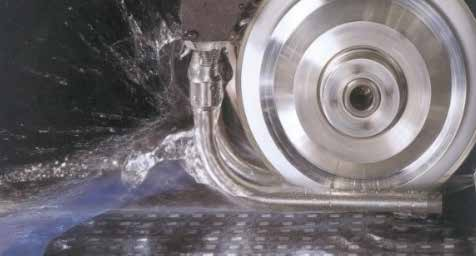
During blade dicing, water is supplied to cool the processing point and remove cutting particles. The specific coolant arrangement is matched to the machine and application.
Bond development for silicon and compound semiconductors
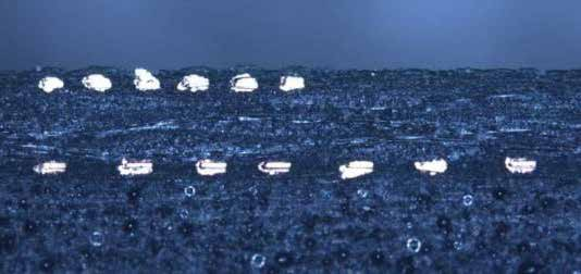
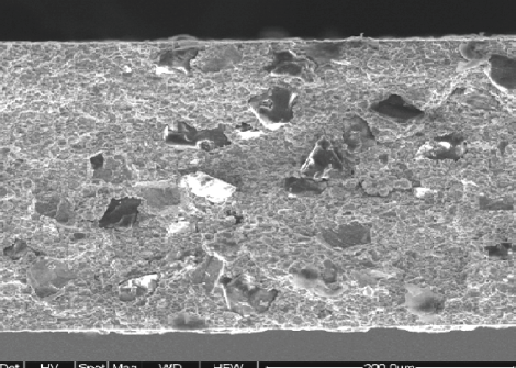
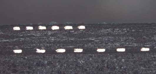
EHWA describes a bond development for silicon and compound semiconductors. The objectives are small top-side and backside chips and improved productivity through suitable high feed rates. The document illustrates these objectives with two cut images:
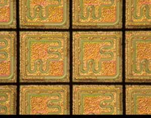
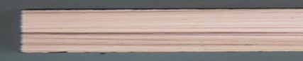
BSL CMP conditioners: diamond retention and pad surface

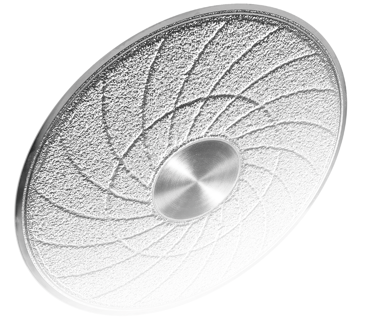
BSL combines mechanical contact and chemical bonding to retain diamonds. EHWA describes a carbide interface between diamond and bond material as a contribution to corrosion resistance. Using the diamond edges supports long useful life. High diamond exposure creates space for removed pad material and supports conditioning efficiency and debris removal.
Proprietary brazing technology and controlled diamond orientation support a high, sustained Pad Cut Rate (PCR) and the required pad roughness. PCR describes removal from the pad. It is distinguished from the removal rate on the wafer.
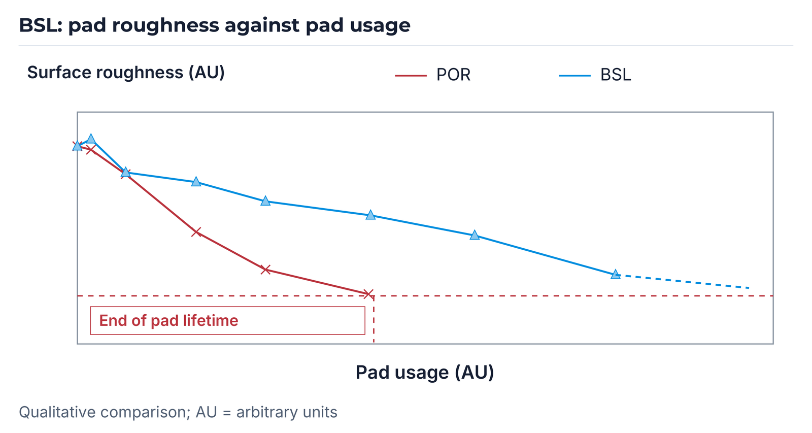
The qualitative comparison shows pad usage and surface roughness in arbitrary units (AU). In the illustrated example, BSL maintains pad roughness above the lifetime threshold longer than the comparison curve labelled POR.
A long-lasting BSL conditioner can support longer pad use, higher CMP equipment availability and fewer pad changes. This creates the potential for lower cost of consumables (CoC). The effect is considered together with the pad, slurry and CMP process.
CVD CMP conditioners: design geometry and process performance
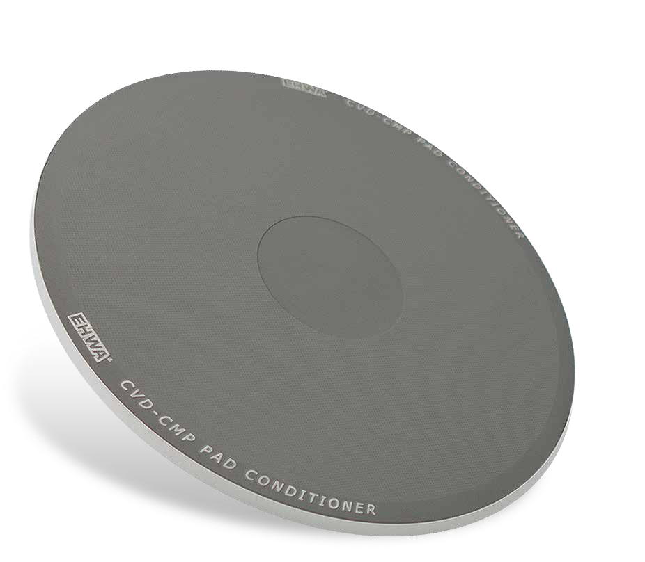
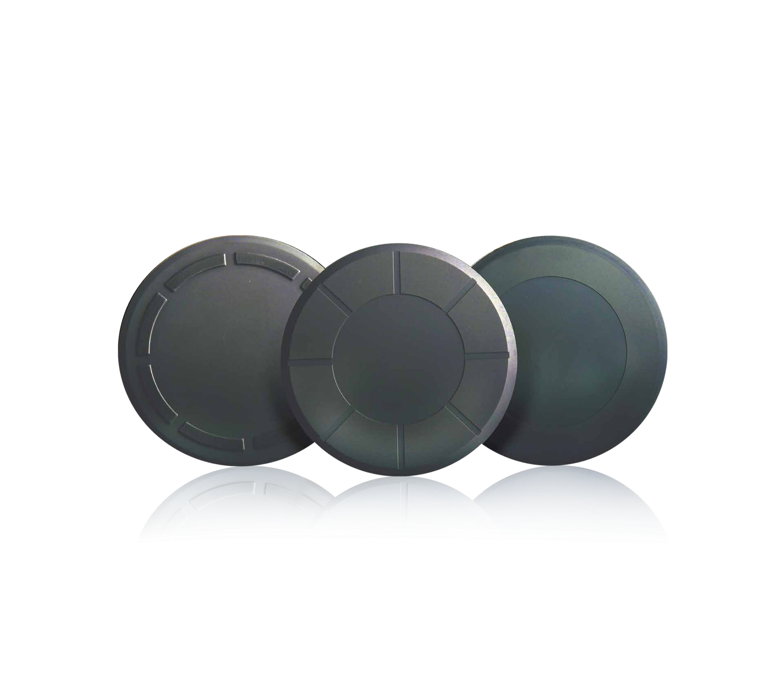
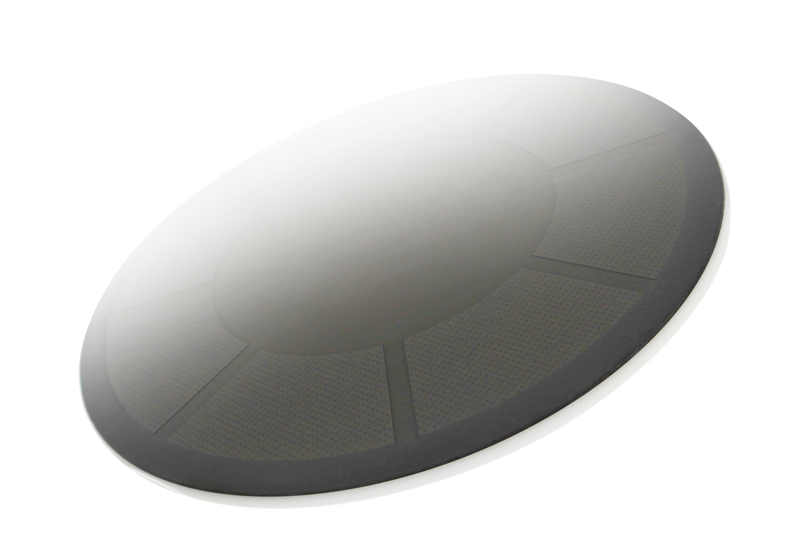
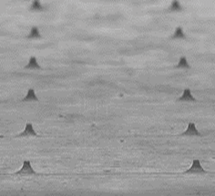
Under the principle of engineered quality control, EHWA identifies the following properties:
- A chemically stable, inert diamond surface.
- Good disk flatness with uniform tip size and exposure.
- Adjustment of Pad Cut Rate (PCR) and Wafer Removal Rate (WRR) through tip geometry, exposure and shape.
- Consistent PCR and WRR sustained over polishing time as a design objective.
WRR here describes material removal from the wafer; PCR describes removal from the pad. Both parameters are influenced by the conditioner structure.
Diamond-coated tips can be arranged in different patterns. Flat contact faces at the tip apex and the tip design allow the load applied to each tip to be adjusted. EHWA refers to patents concerning tip size and number in the technical document.
Contact geometry retained over conditioning time can support consistent PCR. Selection therefore considers the contact area, number and distribution of working tips as well as the diamond coating.
Ring, pellet and bar designs for CMP
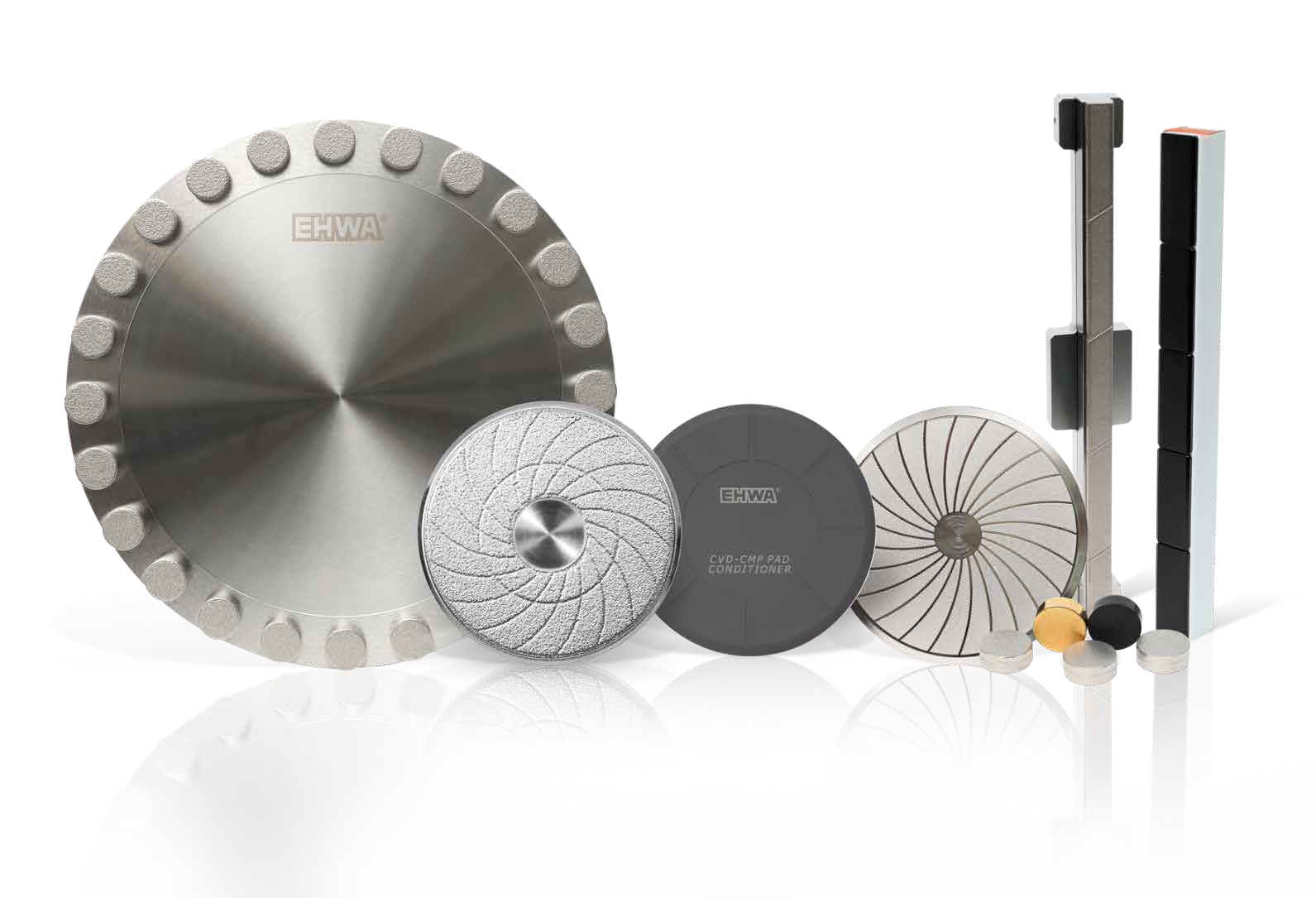
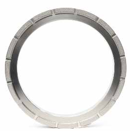
EHWA describes BSL and CVD technologies for large conditioning disks, bar forms, ring forms and designs for legacy CMP tools. The geometry is matched to the existing tool.
Proprietary brazing powders and high-temperature/vacuum brazing support strong diamond retention. EHWA describes the connection as a dual bonding mode: mechanical retention and chemical bonding.
Image comparison of diamond retention
| Conditioner in the image comparison | Reported operating time | Image observation reported by EHWA |
|---|---|---|
| Electroplated disk | 20 h | Heavy diamond loss observed |
| EHWA BSL disk | 60 h | No diamond loss observed |


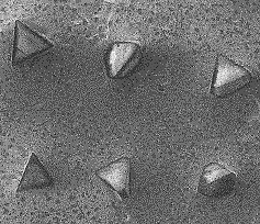
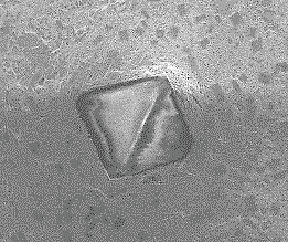
The images show different operating times; further comparison conditions are not specified.
Uniform tip height and multiple pad cycles
BSL brazing and orientation technology supports sustained PCR. For CVD, EHWA qualitatively describes very small (“near-zero”) tip-height variations to reduce wafer defects and unwanted topography. Customised tip configurations allow adjustment of PCR, pad roughness and Material Removal Rate (MRR) on the wafer.
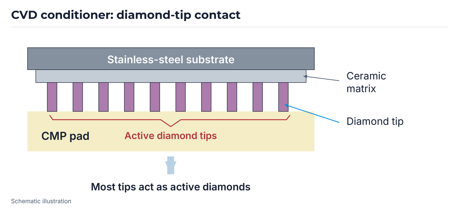
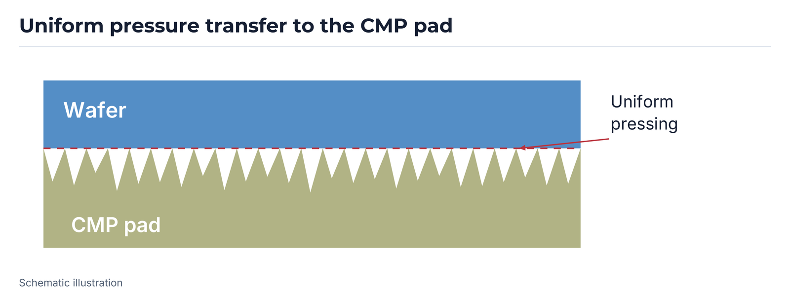
Low diamond wear can enable a CVD conditioner to be used across several pads and lower cost of consumables per wafer. EHWA also identifies the CVD technology as pad conditioning for high MRR in SiC CMP and as a Process of Record (POR). The design is matched to the particular SiC process.
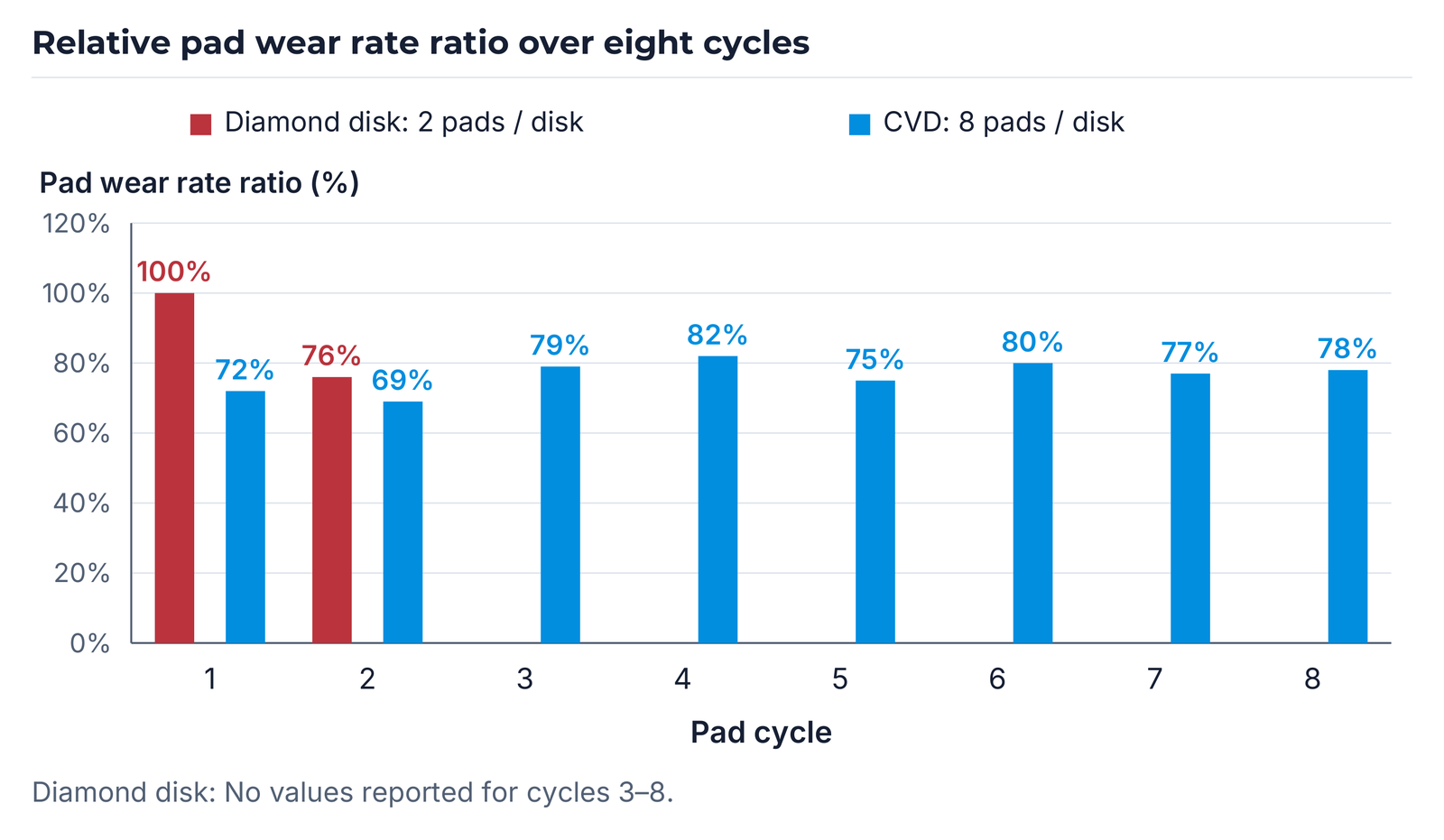
| Pad cycle | Diamond disk: relative pad wear rate ratio | CVD disk: relative pad wear rate ratio |
|---|---|---|
| 1 | 100% | 72% |
| 2 | 76% | 69% |
| 3 | no value shown | 79% |
| 4 | no value shown | 82% |
| 5 | no value shown | 75% |
| 6 | no value shown | 80% |
| 7 | no value shown | 77% |
| 8 | no value shown | 78% |
The example shows two pads per diamond disk and eight pads per CVD disk. The percentages describe the relative pad wear rate ratio; no diamond-disk values are given for cycles 3–8. Pad life and replacement intervals are matched to the specific CMP process.
Discuss your semiconductor application
For back grinding and dicing, useful information includes material structure, wafer/package dimensions, machine, mounting, current tool specification and required quality. Add known feed rates, rotational speeds, coolant arrangements and observed chipping.
For CMP, the tool type, pad, slurry, existing conditioner, PCR, wafer removal rate, surface requirements and replacement intervals are useful. Available information is enough to start; further details can be developed in the technical discussion.
EHWA Europe: info@ehwadia.de · +49 6173 997780
Editorial edition: 13 October 2026. Technical basis: EHWA, Semiconductor.