CMP conditioning and wafer edge grinding
Engineered contact areas in CMP and stable profiles for wafer edges support two different semiconductor manufacturing steps. This programme combines CVD diamond conditioners, BSL double-layer and electroplated conditioners, and profile grinding tools for silicon and sapphire wafers.
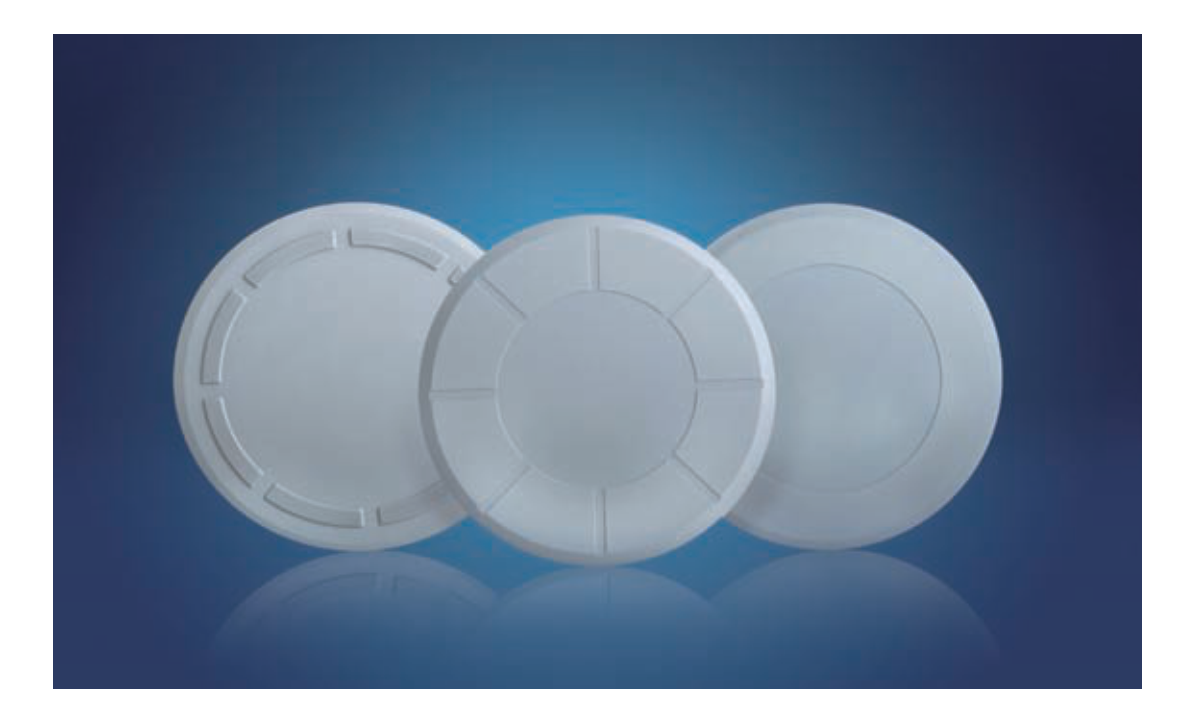
In CMP, the conditioner activates the polishing pad surface. PCR (Pad Cut Rate) describes removal from the pad; WRR (Wafer Removal Rate) describes removal from the wafer. Both are matched with pad, slurry and equipment settings. Edge grinding focuses on chamfer width, groove profile, profile retention and the division between rough and fine grinding. The product images illustrate tool forms and applications.
CVD: engineered tips and effective contact areas
CVD conditioners use chemical vapor deposition to coat a patterned surface with diamond. This construction differs from individual diamond grains held by electroplated nickel or brazing. The tip pattern is engineered for the respective CMP process.
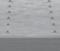
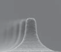
Uniform tip size and protrusion support flatness of the effective contact surface. A flat tip apex allows local loading to be engineered. Tip size, number, shape, pattern and protrusion influence PCR and wafer removal. In the illustrated conditioning concept, the engineered tip shape remains largely consistent over use, supporting stable contact conditions and conditioning action. EHWA also describes this development in its patent publications on tip and contact-area design.
The CVD surface provides high chemical stability. Its diamond-coated working surface can reduce exposure of metallic bonding material to process chemistry. The product sheets describe this benefit as avoiding corrosion and metal contamination. The selected disc is matched to the slurry actually used.
Customisation considers the polished material, pad and slurry. The application matrix lists oxide CMP with ceria-/silica-based slurry and tungsten and copper CMP, each with bulk and barrier steps. Closed-cell and open-pore pads are marked as application areas in all five process columns.
| Design feature | Benefit in the conditioning concept |
|---|---|
| Various tip patterns | Customisation for the respective CMP process |
| Flat tip apex | Engineered contact area |
| Pressure per tip | Control of local pad loading |
| Tip size and number | Patent-related development of contact design |
| Consistent tip shape | Stable contact conditions over use |
| Consistent PCR | Stable conditioning action in the intended process |
| Pad | Oxide CMP: ceria/silica | W CMP: bulk | W CMP: barrier | Cu CMP: bulk | Cu CMP: barrier |
|---|---|---|---|---|---|
| Closed-cell | ● | ● | ● | ● | ● |
| Open-pore | ● | ● | ● | ● | ● |
CVD product ranges and customisation
The CVD product sheets specify an outside diameter of 2–5 inches. Tip size, number and height are customised within the stated ranges. Height is determined according to tip size. These specifications belong to the programme described in the product sheets and provide a basis for application engineering.
A flat apex and engineered tip pattern allow the effective contact area to be tailored. The resulting load per tip is an important design variable. The objective is a sufficiently active pad surface with consistent roughness and economical pad consumption.
| Feature | Range stated in product sheet |
|---|---|
| Outside diameter | 2–5 inches |
| Tip size | Customised, over 5 µm |
| Tip number | Customised, below 30,000 per disc |
| Tip height | Customised, below 100 µm; determined by tip size |
Consistent conditioning through pad use
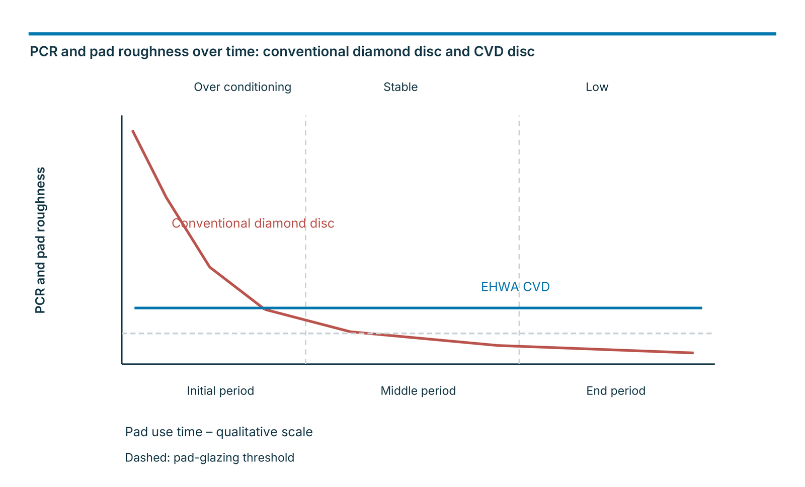
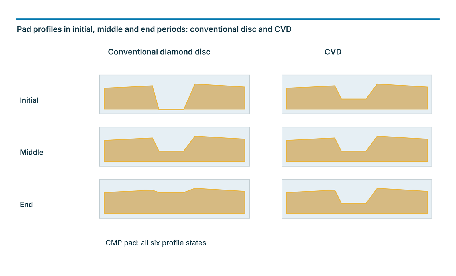
The product sheets compare a conventional diamond disc and a CVD disc over time. In the conventional design, PCR and pad roughness decline considerably in the illustrated trend: strong initial conditioning is followed by a stable middle period and finally low conditioning action. The CVD line remains above the indicated pad-glazing threshold in the model.
The six corresponding pad profiles illustrate the different action in initial, middle and end periods. The conventional profile changes from a deep cut to a shallower contact profile; the CVD profiles remain similar across the three stages. The diagrams describe a qualitative comparison without numerical time or roughness values.
Uniform tip shape and contact area support process stability over use. Controlled conditioning aims to limit both excessive initial pad cutting and insufficient activation towards the end. This can extend the period during which a disc operates within a suitable working range.
BSL double-layer and electroplated conditioners
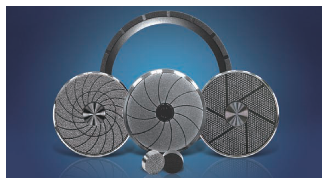
In the BSL design, chemical reaction and mechanical contact hold the diamond to the substrate. Strong grain retention provides a basis for reliable pad conditioning. A carbide layer at the interface between diamond and metallic substrate supports corrosion resistance.
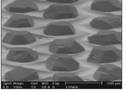
The usable edges of the diamond faces enable an extended effective working life of the grain. High protrusion and generous chip pockets support conditioning and removal of pad debris. The programme includes the new BSL double metal layer design and electroplated variants; the microstructural images show their different diamond arrangements. Selection considers pad, slurry and the required conditioning action.


BSL double-layer and electroplated variants: applications and product data
The application overview includes oxide CMP with BPSG, TEOS and PSG, metal CMP with aluminium, tungsten and copper, and STI, PGI, poly-Si and TSV CMP with Cu or poly-Si. These application groups are listed jointly for the conditioner programme.
The equipment list names AMAT, Ebara, Novellus, Strasbaugh and Lam models, as well as other equipment. The stated PCR range is 10–300 µm/h. Tool design and mounting are selected for the specific machine.
| Application group | Named materials / processes |
|---|---|
| Designs | New BSL double metal layer; electroplated design |
| Oxide CMP | BPSG, TEOS, PSG |
| Metal CMP | Al, W, Cu |
| Further processes | STI, PGI, poly-Si; TSV CMP → Cu, poly-Si |
| Manufacturer | Models listed in product sheet |
|---|---|
| AMAT | Mirra / Reflexion |
| Ebara | F-Rex200/300; EPO-222(H) |
| Novellus | Auriga; CMP200/300; Avantgaard 776 (676); Momentum |
| Strasbaugh | 6DS-SP; 6ED |
| Lam | Teres |
| Other equipment | Additional models subject to application engineering |
| Pad cut rate of the described programme | 10–300 µm/h |
Defect control: POR and EHWA compared
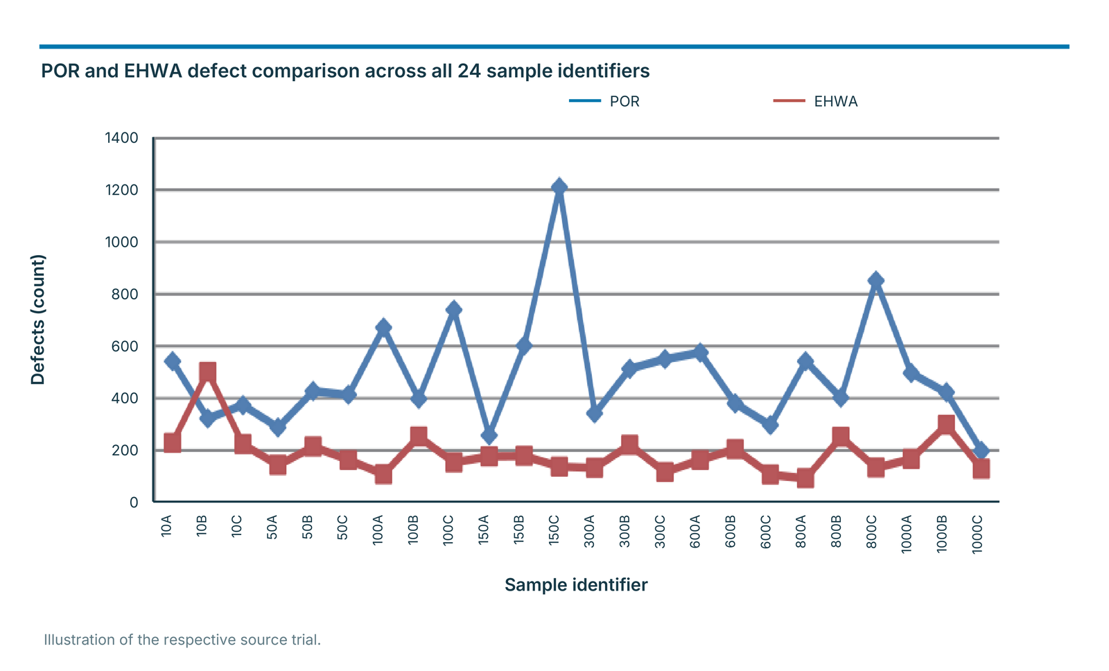
The comparison plots defect counts for POR and EHWA across 24 sample identifiers: 10A/B/C, 50A/B/C, 100A/B/C, 150A/B/C, 300A/B/C, 600A/B/C, 800A/B/C and 1000A/B/C. The blue POR series and red EHWA series remain distinct. The count scale runs from 0 to 1,400.
The EHWA series is lower for most identifiers shown. This example illustrates the potential of appropriate conditioning to support defect control. As complete process conditions are not specified, the comparison applies to the dataset shown.
Tools for silicon and sapphire wafer edges
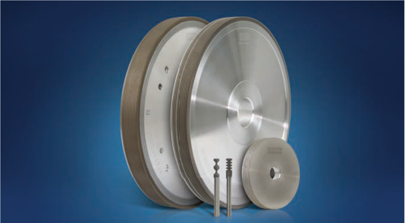
Different groove shapes allow tools to be engineered for different wafer edges. High tool rigidity supports uniform chamfer width. Good groove-profile retention stabilises the edge shape during machining. One tool can be designed for multiple rough and fine grinding stages.
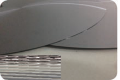
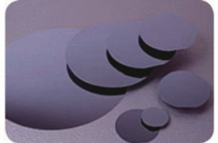
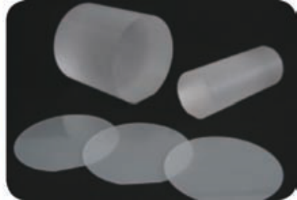
The tool group shows profile grinding wheels and shank tools. Applications include edge grinding of silicon and sapphire wafers. The workpiece images show wafers, a wafer stack and sapphire stock forms. The product table does not specify a diameter unit; diameter and groove form are confirmed during tool selection. The two groove columns list the same identifiers.
| Type | Diameter | Groove (1) | Thickness [mm] | Grit size | Groove (2) |
|---|---|---|---|---|---|
| MD-DW | Ø3.9 | 5G | 5–20 | #325–#3000 | 5G |
| MD-1FF6Y | Ø202 | 8G | 5–20 | #325–#3000 | 8G |
Surfaces and groove measurements
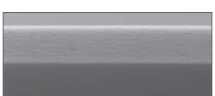
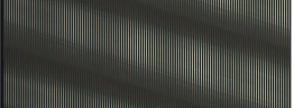
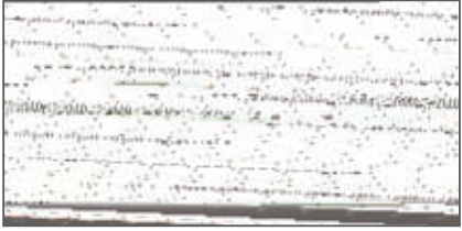
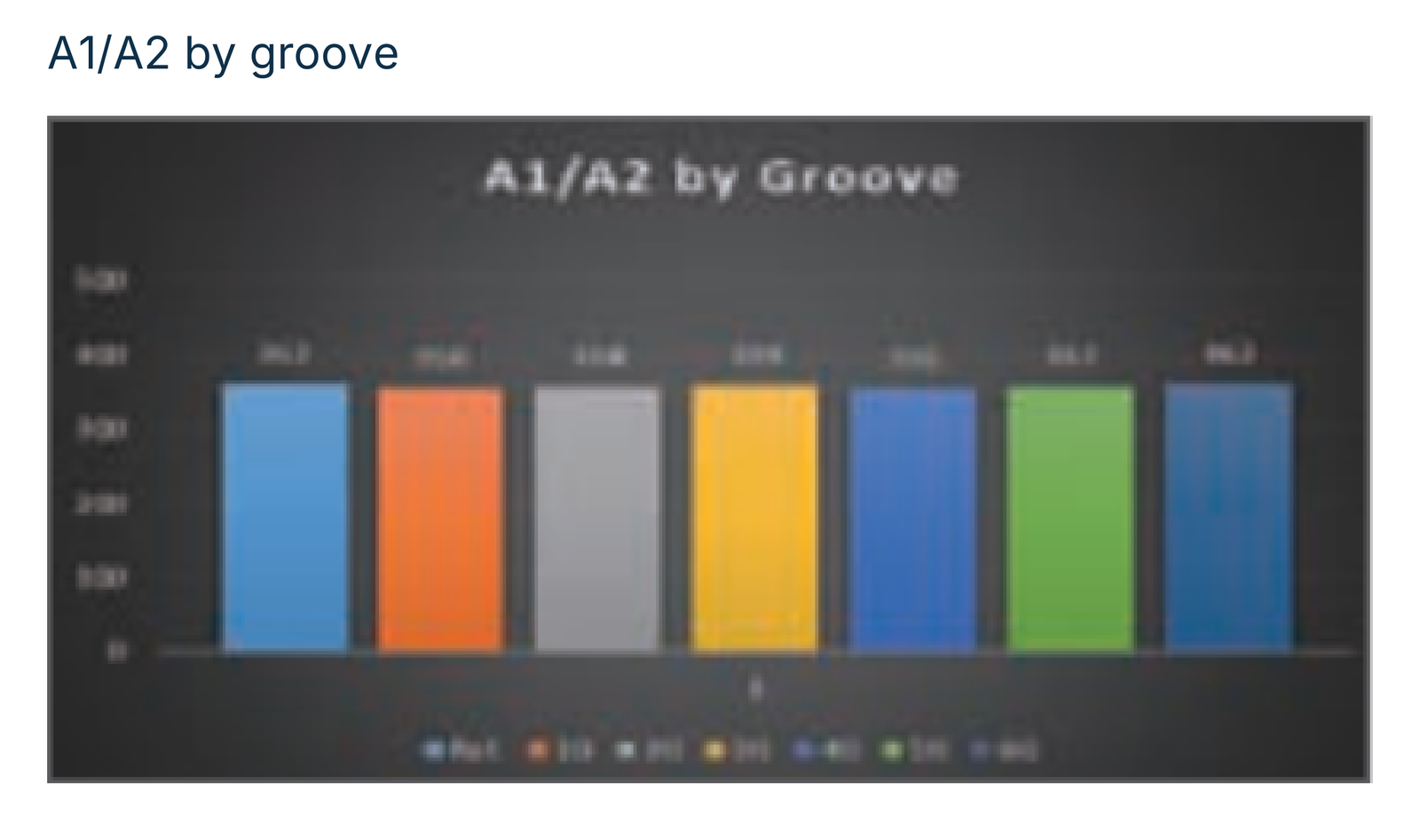
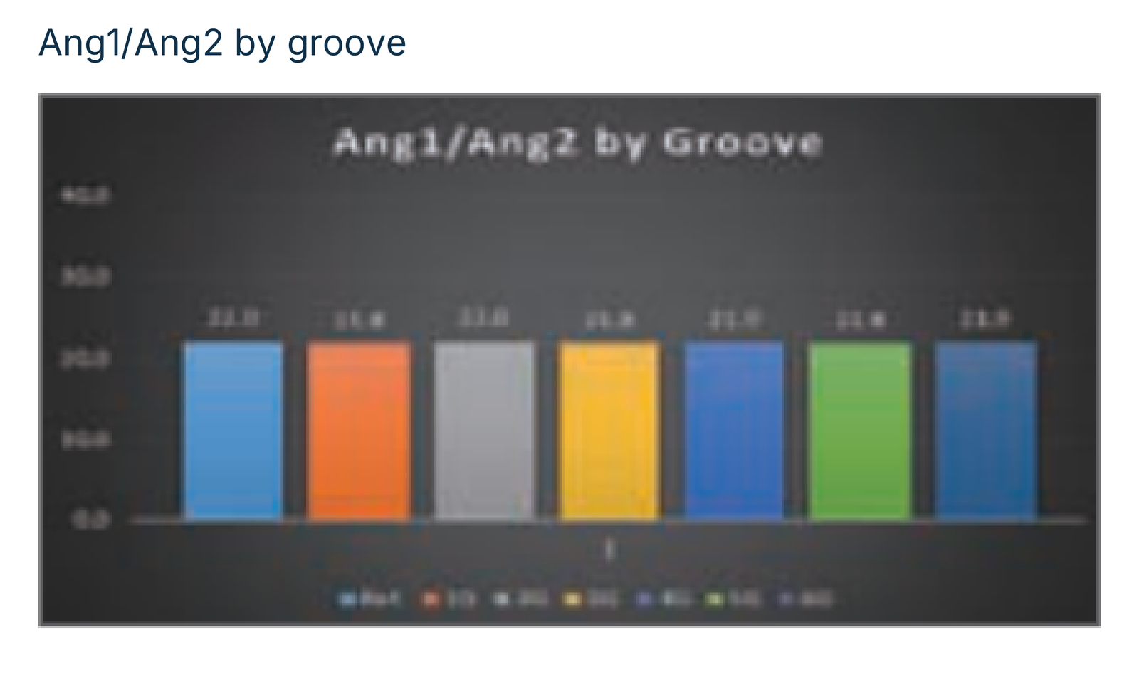
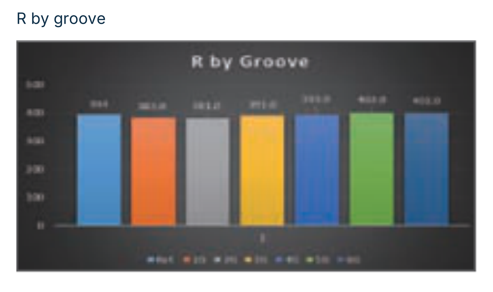
The surface images show sapphire and silicon after edge grinding. An additional measurement image complements the example. Three plots compare A1/A2, Ang1/Ang2 and R by groove against a reference and grooves 1G to 6G. A1/A2 identifies horizontal profile references, Ang1/Ang2 the angular references, and R the radius. These examples support matching the groove profile to the required edge shape. Scales and numerical labels apply to their respective plot; no additional dimensional unit is specified.
Discuss your front-end application
For CMP, machine, mounting, pad, slurry, polished material, PCR and wafer removal data support selection. For edge grinding, include wafer material, dimensions, edge profile and the division between rough and fine grinding. Existing process data or a component drawing provide a starting point. EHWA Europe supports matching the tool design to your process.
Sources and edition
The product sheets carry the print edition 01/2017. This edition was editorially redesigned on 13 October 2026; the editorial date does not represent a new technical approval.
- EHWA: Semiconductor Front End – CVD, CMP and Wafer Edges, pages 1–3 (Q051).
- EHWA: Semiconductor Front End – CVD, CMP and Wafer Edges, pages 1–4 (Q110).
- EHWA: Semiconductor Front End – CVD, CMP and Wafer Edges, pages 1–4 (Q122).
- EHWA: Semiconductor Front End – CVD, CMP and Wafer Edges, pages 1–4 (Q205).
- EHWA: Semiconductor Front End – CVD, CMP and Wafer Edges, pages 1–4 (Q207); identical file to Q205.
EHWA Europe: info@ehwadia.de · +49 6173 997780.