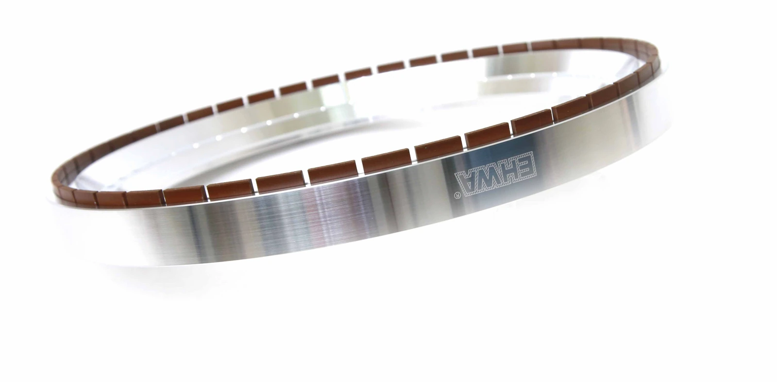
Tools across semiconductor manufacturing
EHWA combines grinding, singulation and CMP pad conditioning with distinct tool families. The starting point is the process task: reducing a wafer to its target thickness, separating devices from a substrate, or preparing a polishing pad surface for a stable CMP process. Each task requires its own tool design and quality criteria.
The EHWA application overviews present back grinding wheels, microblades, dicing blades and diamond pad conditioners. Surface quality, limited edge chipping and economical tool use are central considerations. Tool selection takes account of the material, component structure and machine. A monolithic silicon wafer and a compound structure containing polymer, metal and silicon require different approaches to machining.
Match the process to the tool family
| Manufacturing task | EHWA tool family | Main selection considerations |
|---|---|---|
| Wafer back grinding | Back grinding wheels | Material, target thickness, rough and fine stages |
| Cutting thin substrates or packages | Microblades | Material structure, kerf width, bond |
| Singulating Si and compound semiconductors | Dicing blades | Grit distribution, cutting quality, process control |
| Conditioning a CMP polishing pad | BSL or CVD conditioners | Pad, slurry, diamond arrangement, pad removal |
| Conditioning large or special CMP geometries | Ring, bar and other conditioner designs | Contact geometry, mounting, machine configuration |
This mapping follows the applications shown in the EHWA documents and helps identify the appropriate technical discussion for a particular manufacturing stage. Tools in a multi-stage process should also be considered together. The surface produced by one operation becomes the starting condition for the next.
Designs and process benefits
The back grinding documents distinguish rough and fine grinding. Depending on the tool range, resin, metal or vitrified bonds are used. Material removal, wheel wear and surface requirements are considered together. A suitable design can reduce grinding load and edge chipping while supporting more consistent downstream processing.
Microblades and dicing blades are matched to the material and required kerf. EHWA describes precise thin tool designs, controlled grit distributions and free-cutting performance. These characteristics can support limited chipping, good cutting quality and productive feed rates. The resulting quality is assessed at the top surface, backside and cut edge rather than through a single indicator.
In CMP conditioning, the component being worked on directly is the polishing pad. BSL designs use the bond between the diamond and the surrounding matrix. CVD designs use diamond-coated tips with engineered geometry. The documents describe controlled contact area, adjustment of the pad surface and extended useful life as key development goals. Pad cut rate and material removal rate on the wafer remain different quantities.
Example: A tool chain with distinct functions
The EHWA semiconductor overview presents back grinding, microblade and dicing tools alongside BSL, CVD and ring/pellet conditioners. A back grinding enquiry focuses on the wafer surface; a singulation enquiry focuses on the cut edge; a CMP enquiry concerns the interaction between pad, slurry and conditioner. Keeping those functions distinct also improves the usefulness of a process comparison.
For example, a low grinding current by itself does not identify the best wheel. Similarly, a conditioner delivering a high pad cut rate must be considered alongside pad consumption and the required wafer quality. A useful assessment combines quality, processing time, tool utilisation and the behaviour of the following process stage.
Discuss your application with EHWA
Tell us the manufacturing stage, material structure, machine and quality target. An existing tool specification and information on surface finish, cutting quality or CMP performance provide a useful starting point. For a new task, begin with the information already available and develop the remaining requirements in the technical discussion.
EHWA Europe: info@ehwadia.de · +49 6173 997780
Sources and original documents
- BACK GRINDING WHEEL (RESIN & METAL) · PDF pages 1–6.
- EHWA: Semiconductor tools, Semicon application overview · PDF pages 1–5.